Gigabyte MZ72-HB0 User Manual
Displayed below is the user manual for MZ72-HB0 by Gigabyte which is a product in the Motherboards category. This manual has pages.
Related Manuals

MZ72-HB0
AMD EPYC™ Dual processor motherboard
User Manual
Rev. 1.0

Copyright
© 2020 GIGA-BYTE TECHNOLOGY CO., LTD. All rights reserved.
The trademarks mentioned in this manual are legally registered to their respective owners.
Disclaimer
Information in this manual is protected by copyright laws and is the property of GIGABYTE.
Changes to the specifications and features in this manual may be made by GIGABYTE
without prior notice. No part of this manual may be reproduced, copied, translated, transmitted, or
published in any form or by any means without GIGABYTE's prior written permission.
Documentation Classications
In order to assist in the use of this product, GIGABYTE provides the following types of documentation:
UserManual:detailedinformation&stepsabouttheinstallation,congurationandusethis
product (e.g. motherboard, server barebones), covering hardware and BIOS.
User Guide: detailed information about the installation & use of an add-on hardware or
softwarecomponent(e.g.BMCrmware,rail-kit)compatiblewiththisproduct.
Quick Installation Guide: a short guide with visual diagrams that you can reference easily for
installation purposes of this product (e.g. motherboard, server barebones).
Please see the support section of the online product page to check the current availability of these
documents
For More Information
Forrelatedproductspecications,thelatestrmwareandsoftware,andotherinformation,pleasevisit
our website at: http://www.gigabyte.com.
For GIGABYTE distributors and resellers, additional sales & marketing materials are available from our
reseller portal: http://reseller.b2b.gigabyte.com
For further technical assistance, please contact your GIGABYTE representative or visit
http://esupport.gigabyte.com/ to create a new support ticket.
For any general sales or marketing enquires, you may message GIGABYTE server directly by
email: server.grp@gigabyte.com.

- 3 -
Table of Contents
MZ72-HB0 Motherboard Layout ......................................................................................6
Block Diagram .................................................................................................................8
Chapter 1 Hardware Installation .....................................................................................9
1-1 Installation Precautions .................................................................................... 9
1-2 ProductSpecications .................................................................................... 10
1-3 Installing and Removing the CPU and Heat Sink ........................................... 12
1-4 Installing and Removing Memory ................................................................... 13
1-4-1 8-ChannelMemoryConguration ..........................................................................13
1-4-2 Installing and Removing a Memory Module ..........................................................14
1-4-3 DIMM Population Table .........................................................................................14
1-5 Installing and Removing the M.2 SSD Module ............................................... 16
1-6 Back Panel Connectors .................................................................................. 17
1-7 Internal Connectors ........................................................................................ 18
1-8 Jumper Settings ............................................................................................. 27
Chapter 2 BIOS Setup ..................................................................................................28
2-1 The Main Menu .............................................................................................. 30
2-2 Advanced Menu ............................................................................................. 33
2-2-1 Trusted Computing .................................................................................................34
2-2-2 PSP Firmware Versions ..........................................................................................35
2-2-3 Legacy Video Select ...............................................................................................36
2-2-4 AST2500SuperIOConguration ...........................................................................37
2-2-5 S5 RTC Wake Settings ...........................................................................................40
2-2-6 Serial Port Console Redirection .............................................................................41
2-2-7 CPUConguration ..................................................................................................45
2-2-8 AMI Graphic Output Protocol Policy .......................................................................46
2-2-9 PCI Subsystem Settings .........................................................................................47
2-2-10 USBConguration ..................................................................................................48
2-2-11 NVMeConguration ...............................................................................................50
2-2-12 SATAConguration.................................................................................................51
2-2-13 UEFIPOSTLOGOConguration ...........................................................................52
2-2-14 T1sAuthConguration ...........................................................................................53
2-2-15 NetworkStackConguration ..................................................................................54
2-2-16 AMDMemCongurationStatus .............................................................................55
2-2-17 iSCSIConguration ................................................................................................56
2-2-18 Broadcom BCM57416 10GBASE-T Network Connection ......................................57
2-2-19 VLANConguration ................................................................................................63

- 4 -
2-2-20 MACIPv4NetworkConguration ...........................................................................65
2-2-21 MACIPv6NetworkConguration ...........................................................................66
2-3 AMD CBS Menu ............................................................................................. 68
2-3-1 CPU Common Options ...........................................................................................69
2-3-2 DF Common Options ..............................................................................................74
2-3-3 UMC Common Options ..........................................................................................79
2-3-4 NBIO Common Options ..........................................................................................92
2-3-5 FCH Common Options ...........................................................................................98
2-3-6 NTB Common Options .........................................................................................101
2-3-7 SOC Miscellaneous Control .................................................................................102
2-4 AMD PBS Menu ........................................................................................... 103
2-4-1 RAS ......................................................................................................................104
2-5 Chipset Setup Menu ..................................................................................... 106
2-5-1 North Bridge .........................................................................................................107
2-6 Server Management Menu ........................................................................... 108
2-6-1 System Event Log ................................................................................................110
2-6-2 View FRU Information ..........................................................................................111
2-6-3 BMCNetworkConguration .................................................................................112
2-6-4 IPv6BMCNetworkConguration ......................................................................... 113
2-7 Security Menu .............................................................................................. 114
2-7-1 Secure Boot ......................................................................................................... 115
2-8 Boot Menu .................................................................................................... 117
2-9 Save & Exit Menu ......................................................................................... 119
2-10 ABL POST Codes ........................................................................................ 120
2-10-1 StartProcessorTestPoints .....................................................................................120
2-10-2 Memory test points ...............................................................................................120
2-10-3 PMU Test Points ...................................................................................................120
2-10-4 Original Post Code ...............................................................................................121
2-10-5 CPU test points .....................................................................................................122
2-10-6 Topology test points ..............................................................................................122
2-10-7 Extended memory test point .................................................................................122
2-10-8 Gnb Earlier init ......................................................................................................123
2-10-9 PMU test points ....................................................................................................126
2-10-10 ABL0 test points ...................................................................................................126
2-10-11 ABL5 test points ...................................................................................................126
2-11 Agesa POST Codes ..................................................................................... 130
2-11-1 Universal Post Code .............................................................................................130
2-11-2 [0xA1XX] For CZ only memory Postcodes ...........................................................130
2-11-3 S3 Interface Post Code ........................................................................................133
2-11-4 PMU Post Code ....................................................................................................133
2-11-5 [0xA5XX] assigned for AGESA PSP Module ........................................................133

- 5 -
2-11-6 [0xA9XX, 0xAAXX] assigned for AGESA NBIO Module .......................................136
2-11-7 [0xACXX] assigned for AGESA CCX Module .......................................................138
2-11-8 [0xADXX] assigned for AGESA DF Module ..........................................................139
2-11-9 [0xAFXX] assigned for AGESA FCH Module ........................................................139
2-12 BIOS POST Beep code (AMI standard) ....................................................... 141
2-12-1 PEI Beep Codes ...................................................................................................141
2-12-2 DXE Beep Codes .................................................................................................141
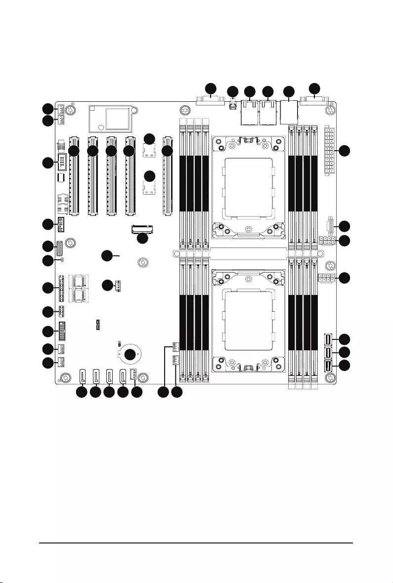
- 6 -
MZ72-HB0 Motherboard Layout
CPU0
CPU1
DIMM_P0_A0
DIMM_P0_B0
DIMM_P0_C0
DIMM_P0_D0
DIMM_P0_H0
DIMM_P0_G0
DIMM_P0_F0
DIMM_P0_E0
DIMM_P1_L0
DIMM_P1_K0
DIMM_P1_J0
DIMM_P1_I0
DIMM_P1_M0
DIMM_P1_N0
DIMM_P1_O0
DIMM_P1_P0
1
2 3 4 5
6
7
8
9
10
11
12
13
14151617181920
22
21
23
24
25
26 27
28 29
30
31
32
33
41
42
34 35 36 37
38
39
40

- 7 -
Item Code Description
1 VGA VGA Port
2 SW_ID ID button with LED
3 LAN1 10GbE Ethernet LAN Port #1
4 LAN2 10GbE Ethernet LAN Port #2
5 USB3_MLAN Server Management LAN Port (Top)/ USB3.0 Ports (Bottom)
6 COM1 Serial Port
7ATX 2 x 12 Pin Main Power Connector
8 PMBUS PMBus Connector
9 P12V_1 2 x 4 Pin 12V Power Connector (for CPU0)
10 P12V_2 2 x 4 Pin 12V Power Connector (for CPU1)
11 SLSAS_0 Slimline Connector #0 (SATAIII 6Gb/s Signal)
12 SLSAS_2 Slimline Connector #2 (SATAIII 6Gb/s Signal)
13 SLSAS_1 Slimline Connector #1 (SATAIII 6Gb/s Signal)
14 CPU1_FAN CPU Fan Connector (for CPU1)
15 CPU0_FAN CPU Fan Connector (for CPU0)
16 SATA_SGP SATA SGPIO Connector
17 SATA3 SATAIII 6Gb/s Connector #3
18 SATA2 SATAIII 6Gb/s Connector #2
19 SATA1 SATAIII 6Gb/s Connector #1
20 SATA0 SATAIII 6Gb/s Connector #0
21 SYS_FAN2 System Fan Connector #2
22 BAT Battery Socket
23 SYS_FAN1 System Fan Connector #1
24 F_USB3 Front Panel USB 3.0 Connector
25 F_USB2 USB 2.0 Header
26 FP_1 Front Panel Header
27 IPMB IPMB Connector
28 CASE_OPEN Case Open Intrusion Alert Header
29 LED_BMC1 BMC Firmware Readiness LED
30 BP_1 HDD Back Plane Board Connector
31 M2_0 M.2 slot (PCIe Gen4 x4, Support NGFF-2280/22110)
32 SPI_TPM TPM Module Connector
33 COM2 Serial Port Cable Connector
34 PCIE_1 PCIe x16 Slot #1 (Gen4 x8)
35 PCIE_2 PCIe x16 Slot #2 (Gen4 x8)
36 PCIE_3 PCIe x16 Slot #3 (Gen4 x16)
37 PCIE_4 PCIe x16 Slot #4 (Gen4 x16)
38 NVME_0 Slimline SAS 4i Connector (NVMe/PCIe Gen4 x4)
39 NVME_1 Slimline SAS 4i Connector (NVMe/PCIe Gen4 x4)
40 PCIE_6 PCIe x16 Slot #6 (Gen4 x16)
43 SYS_FAN4 System Fan Connector #4
44 SYS_FAN3 System Fan Connector #3
- 8 -
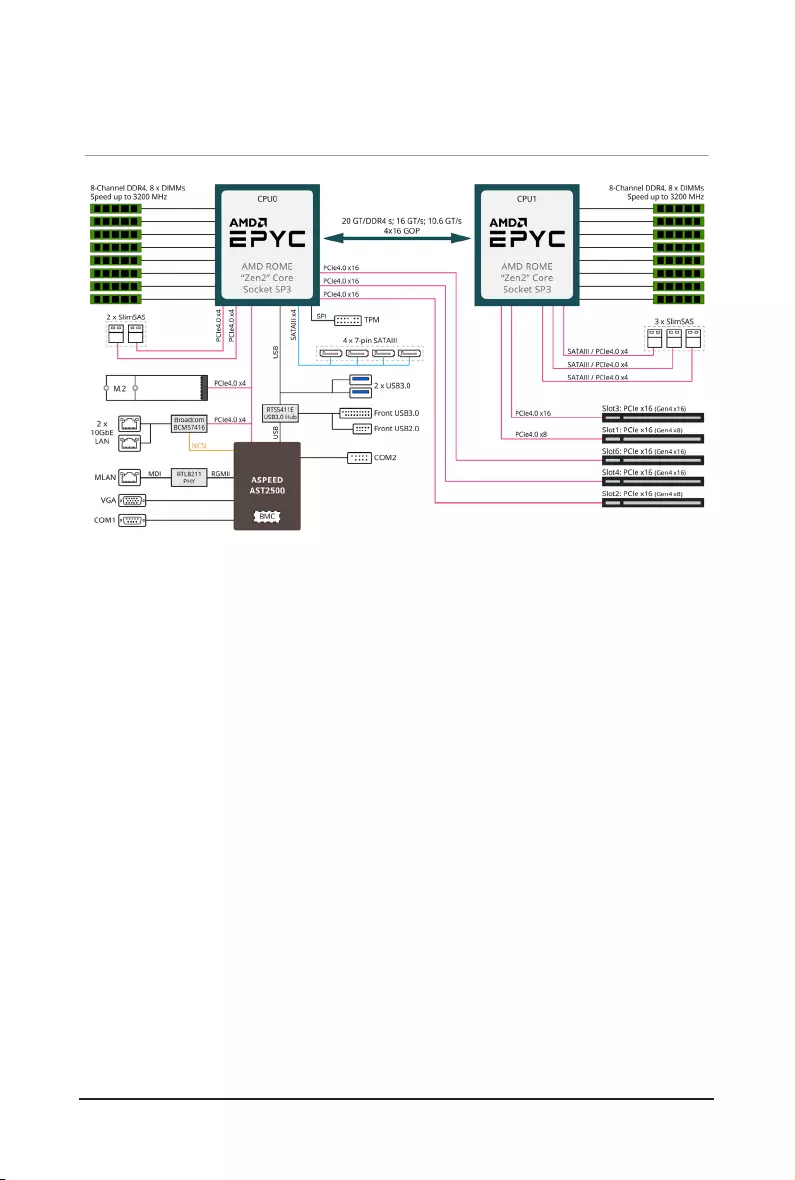
Block Diagram

- 9 - Hardware Installation
1-1 Installation Precautions
The motherboard contains numerous delicate electronic circuits and components which can
become damaged as a result of electrostatic discharge (ESD). Prior to installation, carefully read
the user's manual and follow these procedures:
• Prior to installation, do not remove or break motherboard S/N (Serial Number) sticker or
warranty sticker provided by your dealer. These stickers are required for warranty validation.
• Always remove the AC power by unplugging the power cord from the power outlet before
installing or removing the motherboard or other hardware components.
• When connecting hardware components to the internal connectors on the motherboard,
make sure they are connected tightly and securely.
• When handling the motherboard, avoid touching any metal leads or connectors.
• It is best to wear an electrostatic discharge (ESD) wrist strap when handling electronic
components such as a motherboard, CPU or memory. If you do not have an ESD wrist
strap,keepyourhandsdryandrsttouchametalobjecttoeliminatestaticelectricity.
•
Prior to installing the motherboard, please have it on top of an antistatic pad or within an
electrostatic shielding container.
• Before unplugging the power supply cable from the motherboard, make sure the power
supply has been turned off.
• Before turning on the power, make sure the power supply voltage has been set according to
the local voltage standard.
• Before using the product, please verify that all cables and power connectors of your
hardware components are connected.
• To prevent damage to the motherboard, do not allow screws to come in contact with the
motherboard circuit or its components.
• Make sure there are no leftover screws or metal components placed on the motherboard or
within the computer casing.
• Do not place the computer system on an uneven surface
.
• Do not place the computer system in a high-temperature environment.
• Turning on the computer power during the installation process can lead to damage to
system components as well as physical harm to the user.
• If you are uncertain about any installation steps or have a problem related to the use of the
product,pleaseconsultacertiedcomputertechnician.
Chapter 1 Hardware Installation

Hardware Installation - 10 -
1-2 Product Specications
CPU AMD EPYC™ 7002 series processor family
Dual processors, 7nm, Socket SP3
Up to 64-core, 128 threads per processor
cTDP up to 280W
Chipset System on Chip
Memory 16 x DIMM slots
DDR4 memory supported only
8-Channel memory architecture
RDIMM modules up to 64GB supported
LRDIMM modules up to 128GB supported
Memory speed: Up to 3200/ 2933 MHz
Onboard
Graphics
Integrated in Aspeed® AST2500
2D Video Graphic Adapter with PCIe bus interface
1920x1200@60Hz 32bpp
LAN 2 x 10GbE LAN ports (1 x Broadcom® BCM57416B)
1 x 10/100/1000 management LAN
Expansion Slots Slot_6: 1 x PCIe x16 (Gen4 x16 bus) slot ( from CPU_0)
Slot_4: 1 x PCIe x16 (Gen4 x16 bus) slot ( from CPU_0)
Slot_3: 1 x PCIe x16 (Gen4 x16 bus) slot ( from CPU_1)
Slot_2: 1 x PCIe x16 (Gen4 x8 bus) slot ( from CPU_0)
Slot_1: 1 x PCIe x16 (Gen4 x8 bus) slot ( from CPU_1)
1 x M.2 slot:
- M-key
- PCIe Gen4 x4
- Supports NGFF-2280/22110 cards
2 x U.2 ports:
- SlimSAS 4i type
- PCIe Gen4 x4 per port
Storage Interface 4 x 7-pin SATA 6Gb/s ports
3 x SlimSAS (with 12 x SATA 6Gb/s or 3 x U.2 PCIe Gen4 x4) ports

- 11 - Hardware Installation
Internal I/O
Connectors
1 x 24-pin ATX main power connector
2 x 8-pin ATX 12V power connectors
5 x SlimSAS connectors
1 x M.2 slots
2 x CPU fan headers
4 x System fan headers
1 x USB 3.0 header
1 x USB 2.0 header
1 x COM_2 header
1 x TPM header
1 x Front panel header
1 x PMBus connector
1 x IPMB connector
1xClearCMOSjumper
1xBIOSrecoveryjumper
Rear I/O
Connectors
2 x USB 3.0 ports
1 x VGA port
1 x Serial port
2 x RJ45 ports
1 x MLAN port
1 x ID button with LED
TPM 1 x TPM header with SPI interface
Optional TPM2.0 kit: CTM010
Board
Management
Aspeed® AST2500 management controller
GIGABYTE Management Console (AMI MegaRAC SP-X) web interface
Form Factor E-ATX
305W x 330D (mm)
GIGABYTE reserves the right to makeany changes tothe product specications and product-related
information without prior notice.
Hardware Installation - 12 -
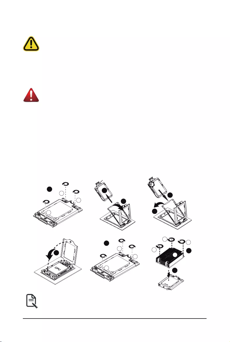
1-3 Installing and Removing the CPU and Heat Sink
Follow these instructions to Install the CPU:
1. Loosen the three captive screws in sequential order (1g2g3) securing the CPU cover.
2. Flip open the CPU cover.
3. Remove the CPU cap with CPU from the CPU frame using the handle on the CPU cap.
4. Using the handle on the CPU cap insert the new CPU cap with CPU installed into the CPU frame.
Note: Ensure that the CPU is installed in the CPU cap in the correct orientation, with the gold triangle
on the CPU aligned to the top left corner of the CPU cap.
5 Flip the CPU frame with CPU installed into place in the CPU socket.
Read the following guidelines before you begin to install the CPU:
• Make sure that the motherboard supports the CPU.
• Always turn off the computer and unplug the power cord from the power outlet before installing
the CPU to prevent hardware damage.
• Unplug all cables from the power outlets.
• Disconnect all telecommunication cables from their ports.
• Placethesystemunitonaatandstablesurface.
• Open the system according to the instructions.
WARNING!
Failure to properly turn off the server before you start installing components may cause serious
damage. Do not attempt the procedures described in the following sections unless you are a
qualiedservicetechnician.
3
3
1
1
2
2
1
External cap
2
3
CPU
4
5
7
1
1
3
3
2
2
6
8
9
3
3
1
1
2
2
44
Note:
• When installing the heatsink to CPU, use T20-Lobe driver to tighten 4 captive nuts in sequence
as 1-4.
• The screw tightening torque: 16.1 ± 1.2 kgf-cm (14.0 ± 1.0 lbf-in).
- 13 - Hardware Installation
1-4 Installing and Removing Memory
Read the following guidelines before you begin to install the memory:
• Make sure that the motherboard supports the memory. It is recommended that memory of the
same capacity, brand, speed, and chips be used.
• Always turn off the computer and unplug the power cord from the power outlet before installing
the memory to prevent hardware damage.
• Memory modules have a foolproof design. A memory module can be installed in only one
direction. If you are unable to insert the memory, switch the direction.
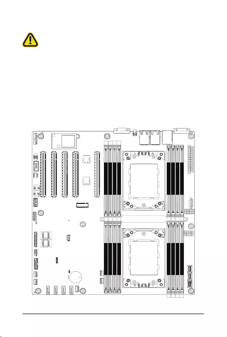
1-4-1 8-Channel Memory Conguration
This motherboard provides 16 DDR4 memory sockets and supports 8-Channel Technology. After the memory
isinstalled,theBIOSwillautomaticallydetectthespecicationsandcapacityofthememory.
CPU0
CPU1
DIMM_P0_A0
DIMM_P0_B0
DIMM_P0_C0
DIMM_P0_D0
DIMM_P0_H0
DIMM_P0_G0
DIMM_P0_F0
DIMM_P0_E0
DIMM_P1_L0
DIMM_P1_K0
DIMM_P1_J0
DIMM_P1_I0
DIMM_P1_M0
DIMM_P1_N0
DIMM_P1_O0
DIMM_P1_P0
Hardware Installation - 14 -
1-4-2 Installing and Removing a Memory Module
Before installing a memory module, make sure to turn off the computer and unplug the
power cord from the power outlet to prevent damage to the memory module.
Be sure to install DDR4 DIMMs on to this motherboard.
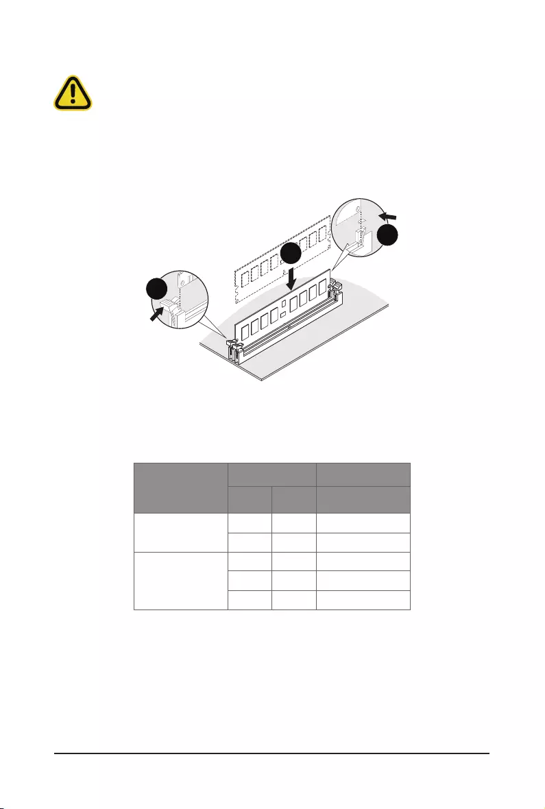
Follow these instructions to install a DIMM module:
1. Insert the DIMM memory module vertically into the DIMM slot and push it down.
2. Close the plastic clip at both edges of the DIMM slots to lock the DIMM module.
3. Reverse the installation steps when you want to remove the DIMM module.
1
2
2
DIMMs Populated
DIMM Frequency (MT/s)
1R 2R
2DR 1.2V
1
1 -- 3200
-- 1 3200
2
2 -- 2933
1 1 2933
-- 2 2933
1-4-3 DIMM Population Table
RDIMM Maximum Frequency Supported Table

- 15 - Hardware Installation
Note:
• 1R: 1 package rank of SDP DRAMs
• 2R: 2 package rank of SDP DRAMs
• 2DR: 2 package rank of DDP DRAMs
• 4DR: 4 package rank of DDP DRAMs
• 1S2R/1S4R/1S8R: 1 package rank of 2/4/8 high 3DS DRAMs
• 2S2R/2S4R/2S8R: 2 package rank of 2/4/8 high 3DS DRAMs
• DIMM must be populated in sequenal alphabec order, starng with bank A.
LRDIMM Maximum Frequency Supported Table
DIMMs Populated
DIMM Frequency (MT/s)
2S2R
2S4R 4DR 1.2V
1
1 -- 3200
-- 1 3200
2
2 -- 2933
1 1 Not Supported
-- 2 2933
3DS RDIMM Maximum Frequency Supported Table
DIMMs Populated
DIMM Frequency (MT/s)
2S2R
2S4R 1.2V
1 1 2933
2 2 2666

Hardware Installation - 16 -
1-5 Installing and Removing the M.2 SSD Module
Follow the steps below to install an optional M.2 SSD module on your motherboard.
Step1. Insert the M.2 SSD module into the slot.
Step2. Secure it with the screw, tightening as necessary to fasten the M.2 SSD module in place.
1
2

- 17 - Hardware Installation
1-6 Back Panel Connectors
uSerial Port
Connects to serial-based mouse or data processing devices.
v10/100/1000 Server Management LAN Port
The LAN port provides Internet connection with data transfer speeds of 10/100/1000Mbps. This port is
the dedicated LAN port for Server Management.
wUSB 3.0 Ports
The USB port supports the USB 3.0 specification. Use this port for USB devices such as a USB
keyboard/mouse,USBprinter,USBashdriveetc.
x10GBASE-T RJ-45 LAN Port #2
The 10 Gigabit Ethernet LAN port provides Internet connection at up to 10 Gbps data rate. See the
section below for a description of the states of the LAN port LEDs.
y10GBASE-T RJ-45 LAN Port #1
The 10 Gigabit Ethernet LAN port provides Internet connection at up to 10 Gbps data rate. See the
section below for a description of the states of the LAN port LEDs.
zID button with LED
Whenthesystemidenticationisactive,theIDLEDonthefront/backpanelglowsblue.
{VGA Port
The video-in port allows connection via video in, which can also apply to the video loop thru function.
v
x y z
{
u
LAN and ID Button LEDs
Link/Activity LED
Speed LED
LAN Port
• Whenremovingthecableconnectedtoabackpanelconnector,rstremovethecablefromyour
device and then remove it from the motherboard.
• When removing the cable, pull it straight out from the connector. Do not rock it side to side to
prevent an electrical short inside the cable connector.
ID button/LED:
10/100/1000 LAN LED:
State Description
Yellow On 1Gbps data rate
Green On 100Mbps data rate
Off 10Mbps data rate
State Description
Blue On Systemidenticationisactive
Off Systemidenticationisdisabled
10GbE LAN LED:
State Description
Yellow On 5Gbps, 2.5Gbps, 1Gps data rate
Green On 10Gbps data rate
Off 100Mbps data rate
w
Hardware Installation - 18 -
1-7 Internal Connectors
Read the following guidelines before connecting external devices:
• First make sure your devices are compliant with the connectors you wish to connect.
• Before installing the devices, be sure to turn off the devices and your computer. Unplug the power
cord from the power outlet to prevent damage to the devices.
• After installing the device and before turning on the computer, make sure the device cable has
been securely attached to the connector on the motherboard.
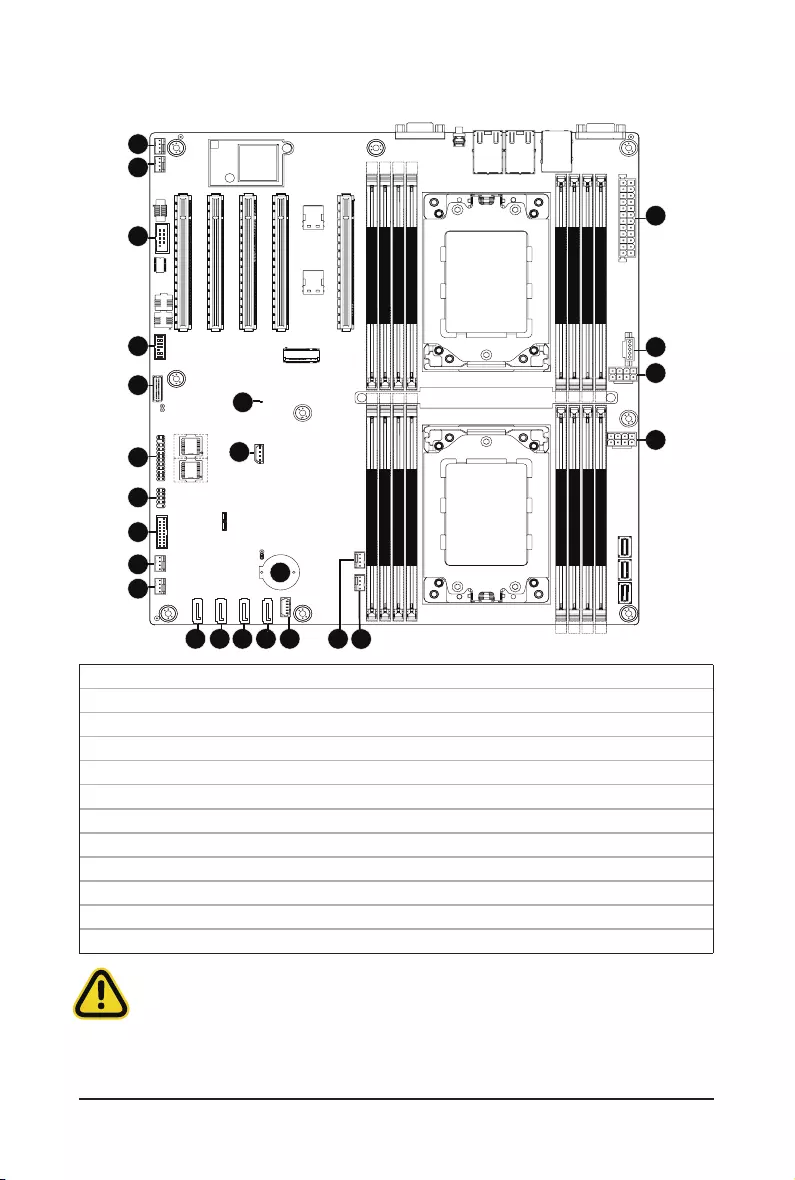
1) ATX 13) SYS_FAN3
2) P12V_1 (for CPU0) 14) SYS_FAN4
3) P12V_2 (for CPU1) 15) PMBUS
4) SATA0 16) F_USB3
5) SATA1 17) F_USB2
6) SATA2 18) COM2
7) SATA3 19) FP_1
8) SATA_SGP 20) BP_1
9) CPU_FAN0 21) SPI_TPM
10) CPU_FAN1 22) IPMB
11) SYS_FAN1 23) LED_BMC1
12) SYS_FAN2 24) BAT
CPU0
CPU1
DIMM_P0_A0
DIMM_P0_B0
DIMM_P0_C0
DIMM_P0_D0
DIMM_P0_H0
DIMM_P0_G0
DIMM_P0_F0
DIMM_P0_E0
DIMM_P1_L0
DIMM_P1_K0
DIMM_P1_J0
DIMM_P1_I0
DIMM_P1_M0
DIMM_P1_N0
DIMM_P1_O0
DIMM_P1_P0
3
4 5 6 78 9 10
11
14
15
16
17
18
19
20
22
21
23
24
13
12
2
1
- 19 - Hardware Installation
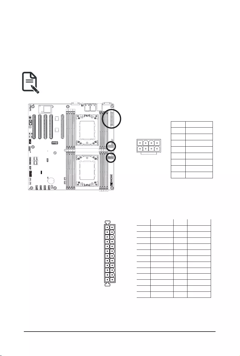
1/2/3) ATX/P12V_1/P12V_2 (2x12 Main Power Connector and 2x4 12V Power Connector)
With the use of the power connector, the power supply can supply enough stable power to all the components
onthemotherboard.Beforeconnectingthepowerconnector,rstmakesurethepowersupplyisturnedoff
and all devices are properly installed. The power connector possesses a foolproof design. Connect the power
supply cable to the power connector in the correct orientation. The 12V power connector mainly supplies
power to the CPU. If the 12V power connector is not connected, the computer will not start.
To meet expansion requirements, it is recommended that a power supply that can withstand high
power consumption be used (500W or greater). If a power supply is used that does not provide the
required power, the result can lead to an unstable or unbootable system.
ATX
P12V_1/ P12V_2
85
41
PinNo. Denition
1 GND
2 GND
3 GND
4 GND
5 +12V
6 +12V
7 +12V
8 +12V
113
1224
Pin No. Denition Pin No. Denition
1 3.3V 13 3.3V
2 3.3V 14 -12V
3 GND 15 GND
4 +5V 16 PS_ON
5 GND 17 GND
6 +5V 18 GND
7 GND 19 GND
8 Power Good 20 -5V
9 5VSB 21 +5V
10 +12V 22 +5V
11 +12V 23 +5V
12 3.3V 24 GND
Hardware Installation - 20 -
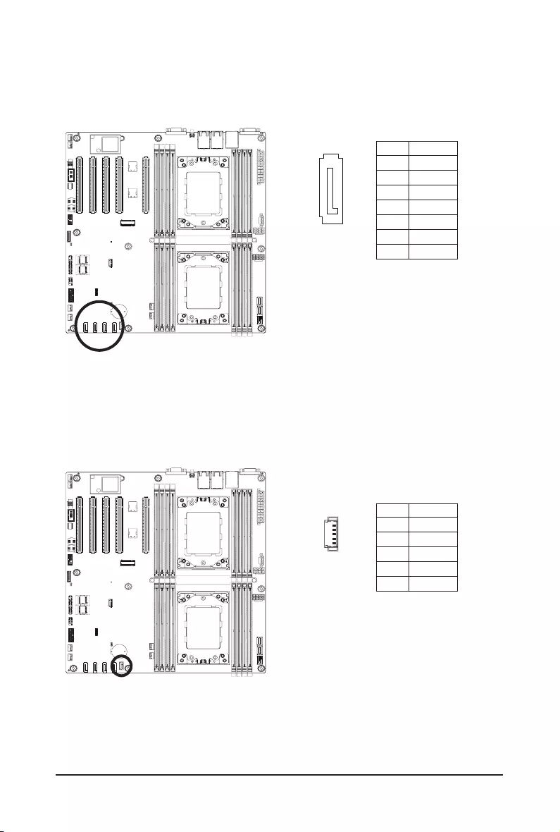
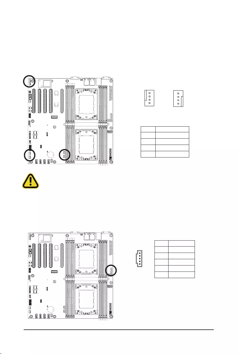
4/5/6/7) SATA0/SATA1/SATA2/SATA3 (SATA 6Gb/s Connectors)
The SATA connectors conform to SATA 6Gb/s standard and are compatible with SATA 3Gb/s standard. Each
SATA connector supports a single SATA device.
PinNo. Denition
1 GND
2 TXP
3 TXN
4 GND
5 RXN
6 RXP
7 GND
1
7
8) SATA_SGP (SATA SGPIO) Connector
Serial General Purpose Input/Output (SGPIO) is a communication method used between a host bus adapter
(HBA) and a main board.
PinNo. Denition
1 Data Out
2 GND
3 Data In
4 Load
5 Clock
1
5
- 21 - Hardware Installation
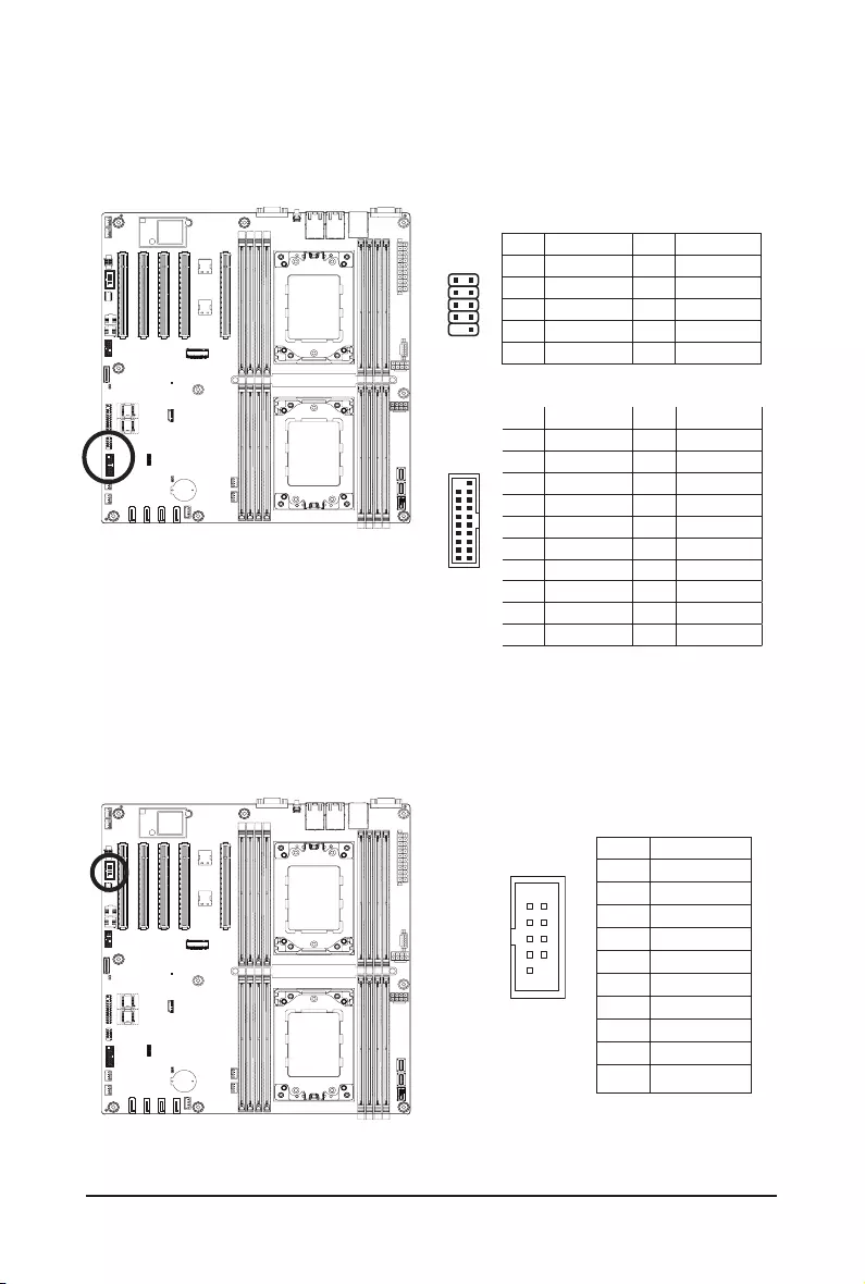
9/10/11/12/13/14) CPU0_FAN//CPU1_FAN/SYS_FAN1/SYS_FAN2/SYS_FAN3/SYS_FAN4 (CPU
FAN/System FAN Headers)
The motherboard has one 4-pin CPU fan header (CPU_FAN), and two 4-pin (SYS_FAN) system fan headers.
Most fan headers possess a foolproof insertion design. When connecting a fan cable, be sure to connect
it in the correct orientation (the black connector wire is the ground wire). The motherboard supports CPU
fan speed control, which requires the use of a CPU fan with fan speed control design. For optimum heat
dissipation, it is recommended that a system fan be installed inside the chassis.
1
1
PinNo. Denition
1 GND
2 +12V
3 Sense
4 Speed Control
• Be sure to connect fan cables to the fan headers to prevent your CPU and system from
overheating. Overheating may result in damage to the CPU or the system may hang.
• Thesefanheadersarenotconfigurationjumperblocks.Donotplacea jumpercaponthe
headers.
4
4
15) PMBus Connector
The Power Management Bus (PMBus) is a variant of the System Management Bus (SMBus) which is
targeted at digital management of power supplies.
5
1
PinNo. Denition
1 PMBus Clock
2 PMBus Data
3 PMBus Alert
4 GND
5 3.3V Sense
Hardware Installation - 22 -
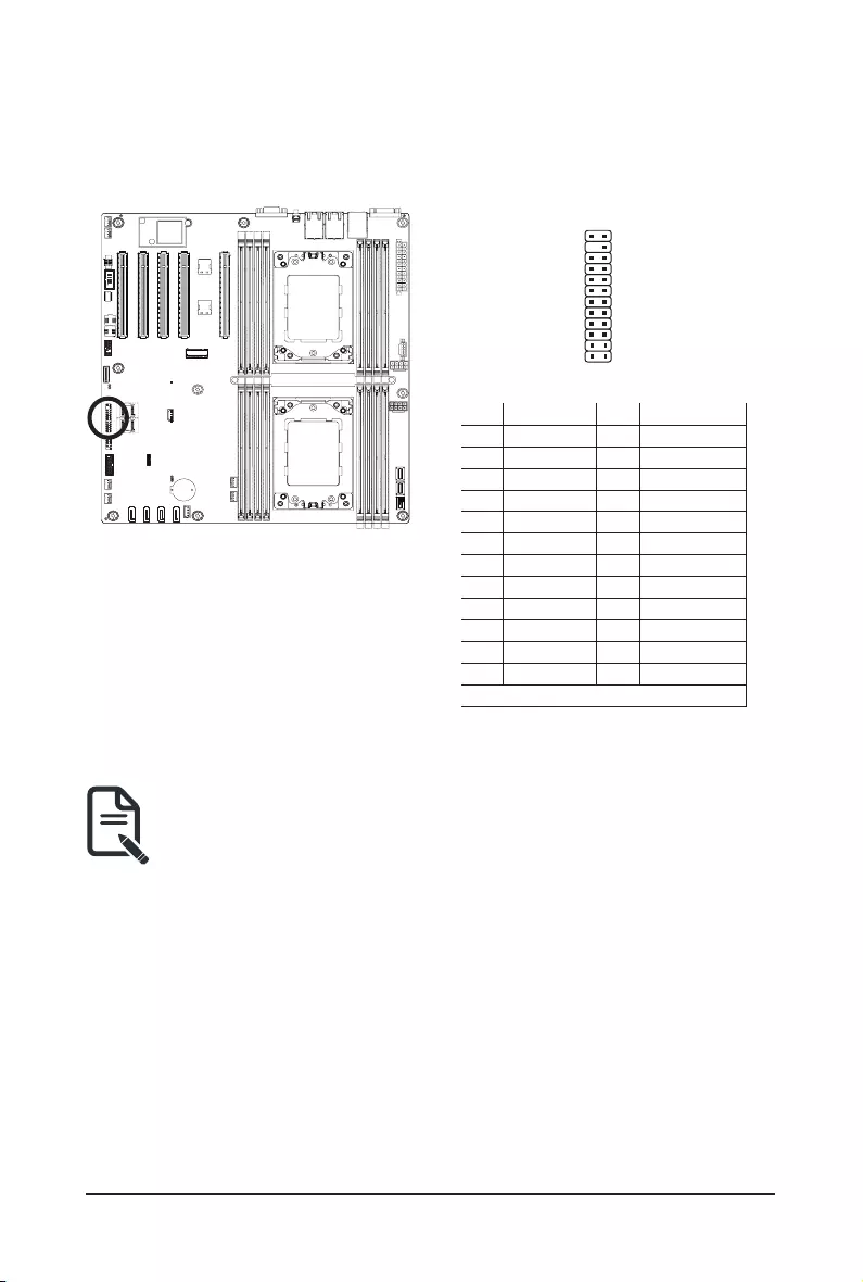
16/17) F_USB3/ F_USB2 (USB 3.0 Connector/ 2.0 Header)
Theconnector/headerconformtoUSB2.0/3.0specication.EachUSBconnector/headercanprovidetwo
USB ports via an optional USB bracket. For purchasing the optional USB bracket, please contact the local
dealer.
USB 2.0 Header
USB 3.0 Connector
Pin No. Denition Pin No. Denition
1 Power 11 IntA_P2_D+
2 IntA_P1_SSRX- 12 IntA_P2_D-
3 IntA_P1_SSRX+ 13 GND
4 GND 14 IntA_P2_SSTX+
5 IntA_P1_SSTX- 15 IntA_P2_SSTX-
6 IntA_P1_SSTX+ 16 GND
7 GND 17 IntA_P2_SSRX+
8 IntA_P1_D- 18 IntA_P2_SSRX-
9 IntA_P1_D+ 19 Power
10 NC 20 No Pin
18) COM2 (Serial Port Cable Connector)
The COM header can provide one serial port via an optional COM port cable. For purchasing the optional
COM port cable, please contact the local dealer.
PinNo. Denition
1 NDCD-
2 NSIN
3 NSOUT
4 NDTR-
5 GND
6 NDSR-
7 NRTS-
8 NCTS-
9 NRI-
10 No Pin
109
21
Pin No. Denition Pin No. Denition
1 Power (5V) 6 USB DY+
2 Power (5V) 7 GND
3 USB DX- 8 GND
4 USB DY- 9 No Pin
5 USB DX+ 10 No Connect
1 2
9 10
120
11 10
- 23 - Hardware Installation
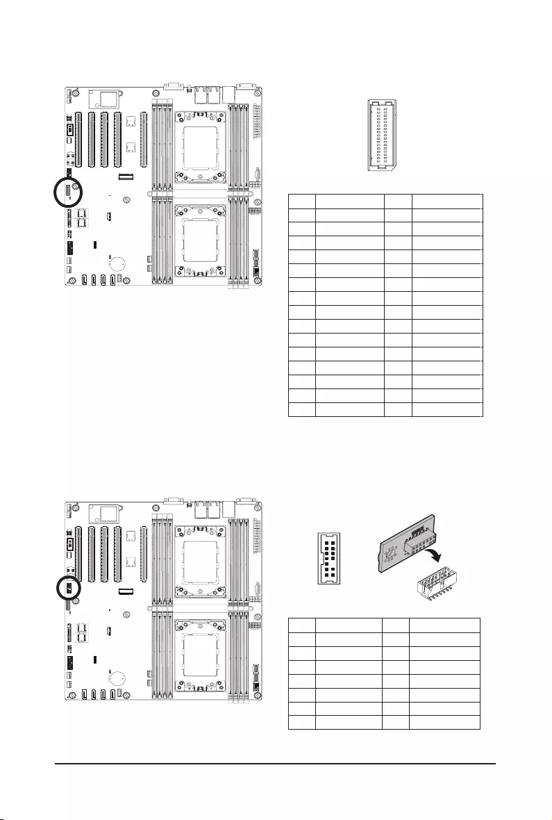
19) FP_1 (Front Panel Header)
Connect the power switch, reset switch, speaker, chassis intrusion switch/sensor and system status indicator
on the chassis to this header according to the pin assignments below. Note the positive and negative pins
before connecting the cables.
The front panel design may differ by chassis. A front panel module mainly consists of power switch,
reset switch, power LED, hard drive activity LED, speaker etc. When connecting your chassis front
panel module to this header, make sure the wire assignments and the pin assignments are matched
correctly.
Pin No. Denition Pin No. Denition
1 Power LED+ 2 5V Standby
3 No Pin 4 ID LED+
5 Power LED- 6 ID LED-
7* HDD LED+ 8 System Status LED+
9* HDD LED- 10 System Status LED-
11 Power Button 12 LAN1 Active LED+
13 GND 14 LAN1 Link LED-
15 Reset Button 16 SMBus Data
17 GND 18 SMBus Clock
19 ID Button 20 Case Open
21 GND 22 LAN2 Actve LED+
23 NMI Switch 24 LAN2 Link LED-
*Note: Pin 7 & Pin 9 are reserved for Gigbate systems.
1
2423
2
Hardware Installation - 24 -
20) BP_1 (HDD Backplane Board Header)
Pin No. Denition Pin No. Denition
1 HP_ALERT_L 2 BPMI DIN/OUT
3 GND 4 BPMI DIN/IN
5 BPMI_LOAD 6 GND
7 BPMI_CLK 8 PLD_Program_EN
9 GLED_AMB_N 10 GLED_GRN_N
11 FAN_IRQ_N 12 Reserved
13 BP_SCL 14 GND
15 BP_SDA 16 BP_RST_N
17 SMB_U2_TMP_SCL 18 GND
19 SMB_U2_TMP_SDA 20 I2C_DEV_RST
21 PH_HP_SCL0 22 GND
23 PH_HP_SDA0 24 GND
25 PH_HP_SCL1 26 GND
27 PH_HP_SDA1 28 GND
15 P3V3_AUX 30 P3V3_AUX
29
30
2 1
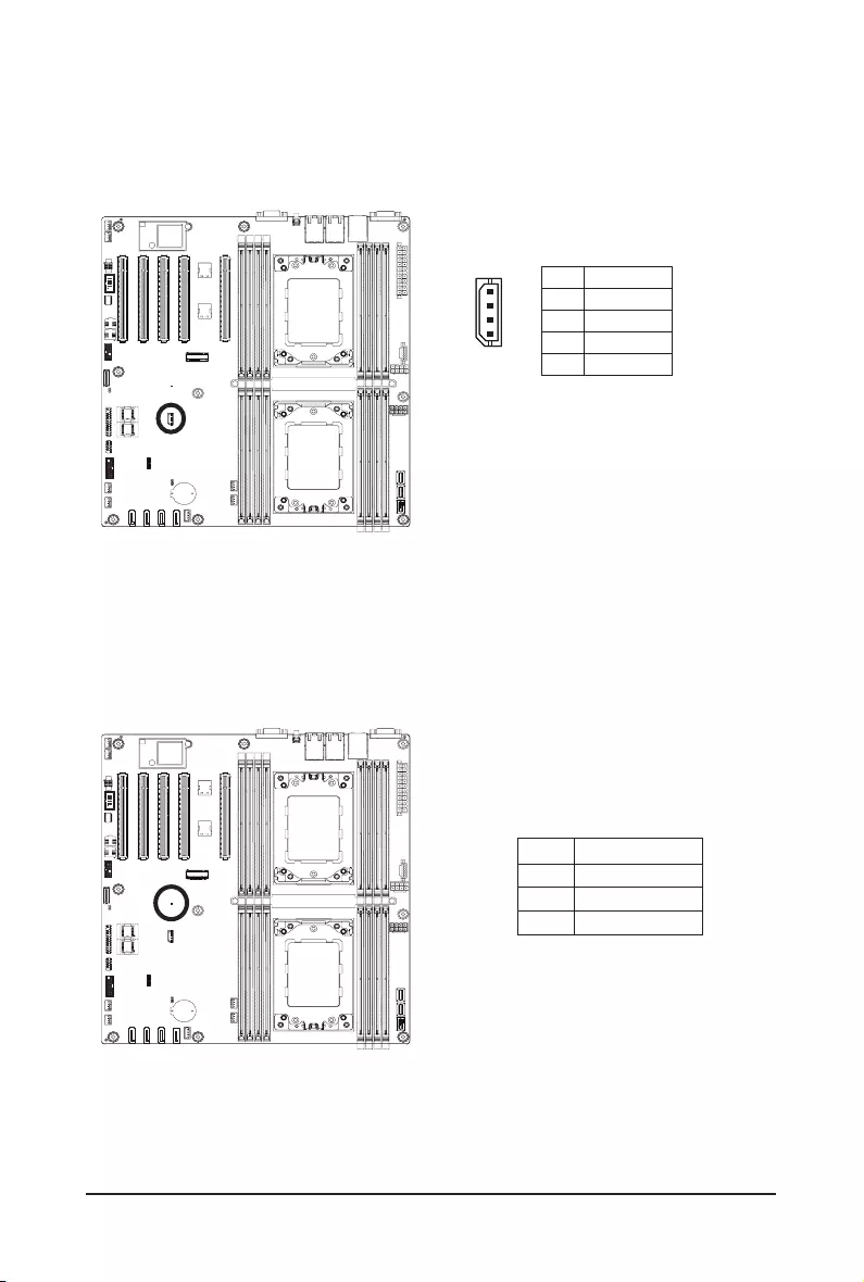
21) SPI_TPM (Trusted Platform Module Connector)
Trusted Platform Module (TPM) is an international standard for a secure cryptoprocessor, a dedicated
microcontroller designed to secure hardware through integrated cryptographic keys.
Pin No. Denition Pin No. Denition
1 Clock 8 No Connect
2 P_3V3_AUX 9 LPC_LAD2
3 LPC_RST 10 No Pin
4 P3V3 11 LPC_LAD3
5 LPC_LAD0 12 GND
6 IRQ_SERIAL 13 LPC_FRAME_N
7 LPC_LAD1 14 GND
12
13 14
- 25 - Hardware Installation
22) IPMB (Intelligent Platform Management Bus) Connector
The Intelligent Platform Management Bus Communications Protocol defines a byte-level transport for
transferringIntelligentPlatformManagementInterfaceSpecication(IPMI)messagesbetweenintelligentI2C
devices.
4
1
Pin No. Denition
1 Clock
2 GND
3 Data
4 VCC
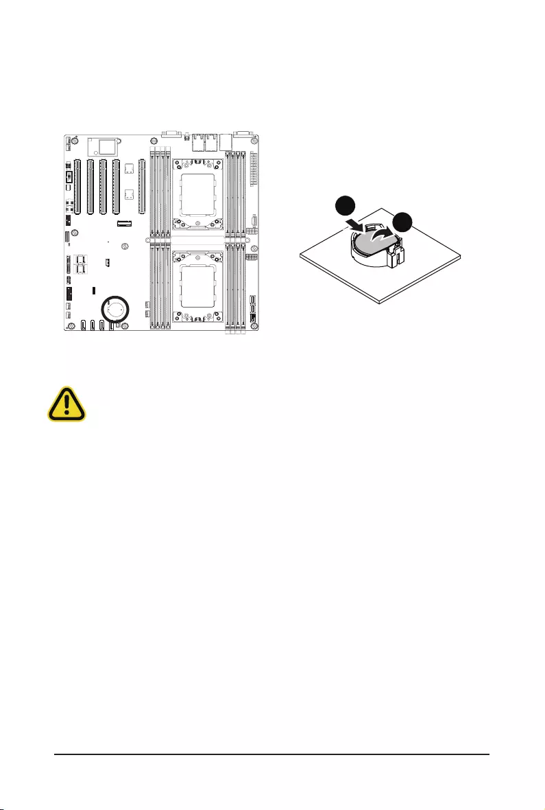
23) LED_BMC (BMC Firmware Readiness LED)
State Description
On BMCrmwareisinitial
Blink BMCrmwareisready
Off AC loss
Hardware Installation - 26 -
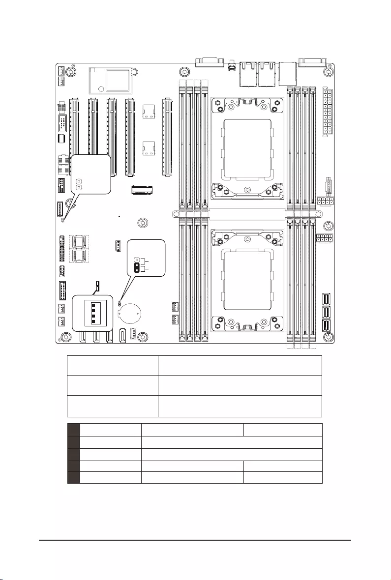
24) BAT (Battery Scoket)
Thebatteryprovidespowertokeepthevalues(suchasBIOScongurations,date,andtimeinformation)in
the CMOS when the computer is turned off. Replace the battery when the battery voltage drops to a low level,
or the CMOS values may not be accurate or may be lost.
• Always turn off your computer and unplug the power cord before replacing the battery.
• Replace the battery with an equivalent one. Danger of explosion if the battery is replaced with an incorrect
model.
• Contact the place of purchase or local dealer if you are not able to replace the battery by yourself or
uncertain about the battery model.
• Used batteries must be handled in accordance with local environmental regulations.
1
2
- 27 - Hardware Installation
1-8 Jumper Settings
Jumper Name Jumper Setting
Chassis Open Intrusion Alert 1-2: Nomal operation (Default)
Clear CMOS 1-2: Nomal operation. (Default)
2-3: Clear CMOS data.
J1 ON OFF
1HSMB_SEL BIOSDened
2N/A BIOSDened
3BIOS PWD Clear Supervisor Password Normal [Default]
4BIOS Recovery BIOS Recovery Mode Normal [Default]
Clear CMOS
CLR_CMOS
Default
Enable
3
2
1
-
21',3
Chassis Open
Intrusion Alert
CASE_OPEN
Case open
GND

BIOS Setup - 28 -
BIOS (Basic Input and Output System) records hardware parameters of the system in the EFI on the
motherboard.ItsmajorfunctionsincludeconductingthePower-OnSelf-Test(POST)duringsystemstartup,
saving system parameters, loading the operating system etc. The BIOS includes a BIOS Setup program that
allowstheusertomodifybasicsystemcongurationsettingsortoactivatecertainsystemfeatures.Whenthe
power is turned off, the battery on the motherboard supplies the necessary power to the CMOS to keep the
congurationvaluesintheCMOS.
To access the BIOS Setup program, press the <DEL> key during the POST when the power is turned on.
Chapter 2 BIOS Setup
• BIOSashingispotentiallyrisky,ifyoudonotencounteranyproblemswhenusingthecurrent
BIOSversion,itisrecommendedthatyoudon'tashtheBIOS. To ash the BIOS, do it with
caution.InadequateBIOSashingmayresultinsystemmalfunction.
• It is recommended that you not alter the default settings (unless you need to) to prevent system
instability or other unexpected results. Inadequately altering the settings may result in system's
failure to boot. If this occurs, try to clear the CMOS values and reset the board to default values.
(Refer to the Exitsectioninthischapterorintroductionsofthebattery/clearingCMOSjumperin
Chapter 1 for how to clear the CMOS values.)
BIOS Setup Program Function Keys
<f><g> Move the selection bar to select the screen
<h><i> Move the selection bar to select an item
<+> Increase the numeric value or make changes
<-> Decrease the numeric value or make changes
<Enter> Execute command or enter the submenu
<Esc> Main Menu: Exit the BIOS Setup program
Submenus: Exit current submenu
<F1> Show descriptions of general help
<F3> Restore the previous BIOS settings for the current submenus
<F9> Load the Optimized BIOS default settings for the current submenus
<F10> Save all the changes and exit the BIOS Setup program

- 29 - BIOS Setup
Main
This setup page includes all the items of the standard compatible BIOS.
Advanced
This setup page includes all the items of AMI BIOS special enhanced features.
(ex:Autodetectfanandtemperaturestatus,automaticallycongureharddiskparameters.)
AMD CBS
ThissetuppageincludesthecommonitemsforcongurationofAMDmotherboard-relatedinformation.
AMD PBS Option
ThissetuppageincludesthecommonitemsforcongurationofAMDCPMRASrelatedsettings.
Chipset
ThissetuppageincludesallthesubmenuoptionsforconguringthefunctionsoftheNorthBridge.
Server Management
Server additional features enabled/disabled setup menus.
Security
Change,set,ordisablesupervisoranduserpassword.Congurationsupervisorpasswordallowsyouto
restrict access to the system and BIOS Setup.
A supervisor password allows you to make changes in BIOS Setup.
A user password only allows you to view the BIOS settings but not to make changes.
Boot
Thissetuppageprovidesitemsforcongurationofthebootsequence.
Save & Exit
Save all the changes made in the BIOS Setup program to the CMOS and exit BIOS Setup. (Pressing
<F10> can also carry out this task.)
Abandon all changes and the previous settings remain in effect. Pressing <Y> to the confirmation
message will exit BIOS Setup. (Pressing <Esc> can also carry out this task.)
BIOS Setup - 30 -
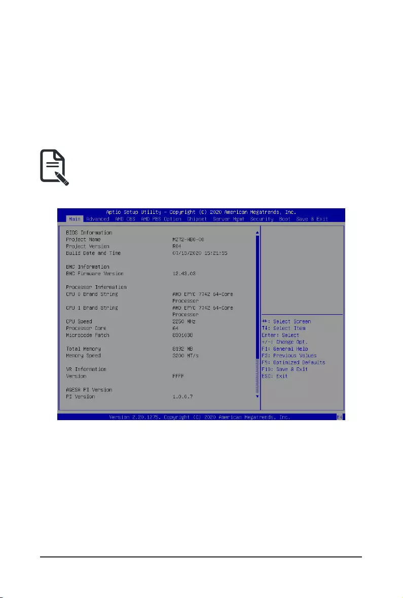
2-1 The Main Menu
Once you enter the BIOS Setup program, the Main Menu (as shown below) appears on the screen. Use
arrow keys to move among the items and press <Enter> to accept or enter other sub-menu.
Main Menu Help
The on-screen description of a highlighted setup option is displayed on the bottom line of the Main Menu.
Submenu Help
While in a submenu, press <F1> to display a help screen (General Help) of function keys available for the
menu. Press <Esc> to exit the help screen. Help for each item is in the Item Help block on the right side of
the submenu.
• When the system is not stable as usual, select the Restore Defaults item to set your system to
its defaults.
• The BIOS Setup menus described in this chapter are for reference only and may differ by BIOS
version.
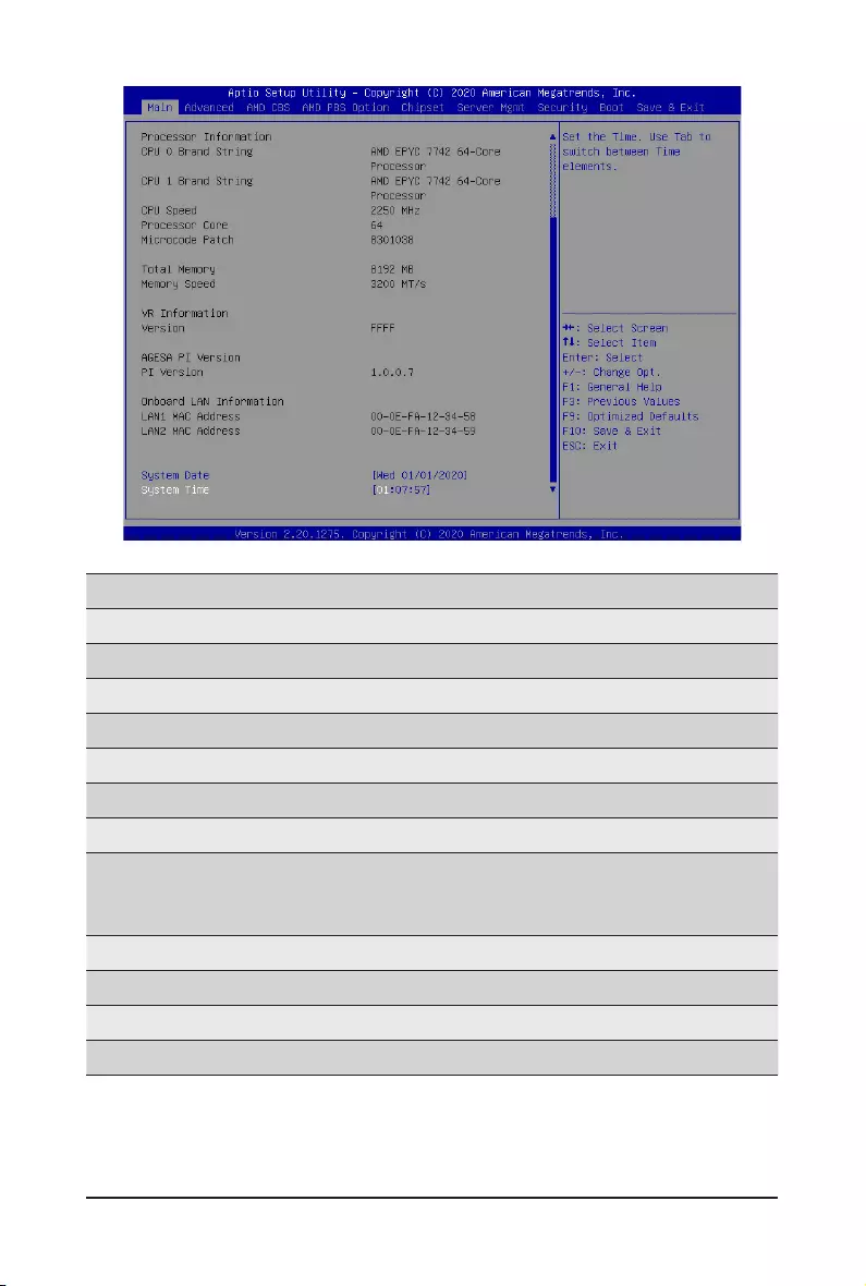
- 31 - BIOS Setup
Parameter Description
BIOS Information
ProjectName Displaystheprojectnameinformation.
ProjectVersion Displays version number of the BIOS setup utility.
Build Date and Time Displays the date and time when the BIOS setup utility was created.
BMC Information(Note1)
BMC Firmware Version(Note1) DisplaysBMCrmwareversioninformation.
Processor Information
CPU0 Brand String/ CPU1 Brand
String/ CPU Speed / Processor
Core / Microcode Patch
Displaysthetechnicalspecicationsfortheinstalledprocessor(s).
Total Memory(Note2) Displays the total memory size of the installed memory.
Memory Frequency(Note2) Displays the frequency information of the installed memory.
VR Information
Version Displays VR version information.
(Note1) Functions available on selected models.
(Note2) This section will display capacity and frequency information of the memory that the customer has
installed.

BIOS Setup - 32 -
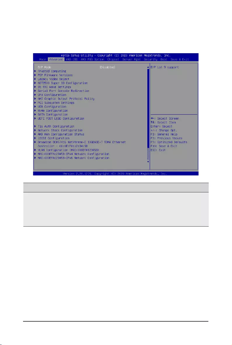
(Note) The number of LAN ports listed will depend on the motherboard / system model.
Parameter Description
AGESA PI Version
PI Version Displays AGESA PI version information.
Onboard LAN Information
LAN1 MAC Address(Note) Displays LAN MAC address information.
LAN2 MAC Address (Note) Displays LAN MAC address information.
System Date Sets the date following the weekday-month-day-year format.
System Time Sets the system time following the hour-minute-second format.
- 33 - BIOS Setup
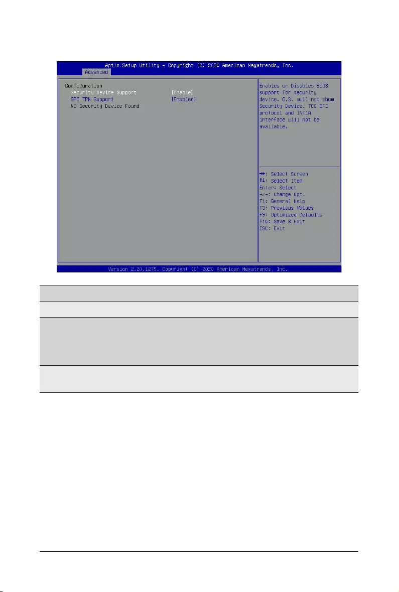
2-2 Advanced Menu
TheAdvancedMenudisplayssubmenuoptionsforconguringthefunctionofvarioushardwarecomponents.
Select a submenu item, then press <Enter> to access the related submenu screen.
Parameter Description
ErP Mode (Energy-related Products)
Enable/Disable ErP Lot 9 support. When ErP Mode is enabled, fan
speedwillbeadjustedandanyredundantPSUwillbeplacedinto
a standby state (“Cold Redundancy”) in order to decrease power
consumption when the server is in idle mode.
Options available: Disabled, Lot 9. Default setting is Disabled.
BIOS Setup - 34 -
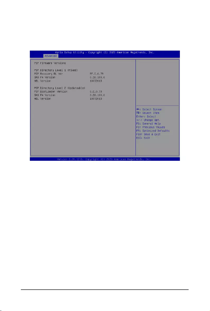
2-2-1 Trusted Computing
Parameter Description
Conguration
Security Device Support
Enable/Disable BIOS support for security device. OS will not show
security device. TCG EFI protocol and INT1A interface will not be
available.
Options available: Enable, Disable. Default setting is Enable.
SPI TPM Support Select Enable to activate TPM support feature.
Options available: Enabled, Disabled. Default setting is Disabled.
- 35 - BIOS Setup
2-2-2 PSP Firmware Versions
ThePSPFirmwareVersionspagedisplaysthebasicPSPrmwareversioninformation.Itemsonthiswindow
arenon-congurable.
BIOS Setup - 36 -
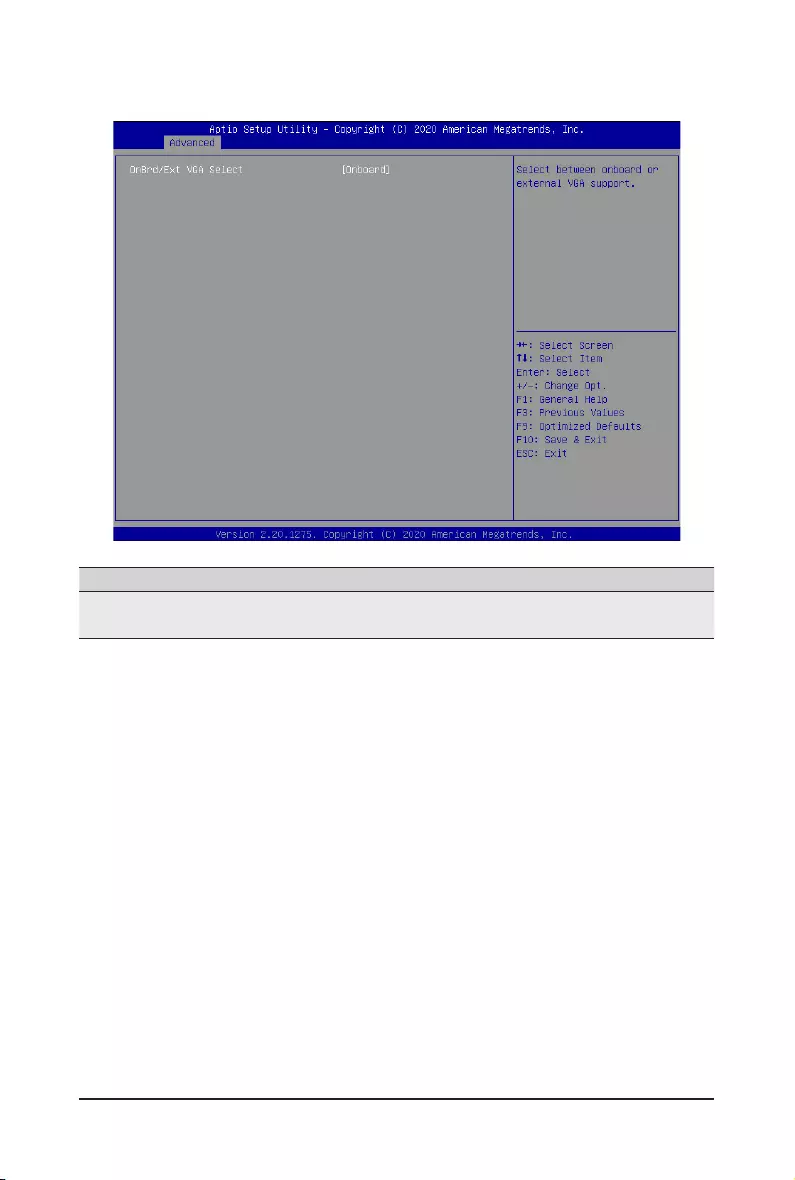
2-2-3 Legacy Video Select
Parameter Description
OnBrd/Ext VGA Select Selects between onboard or external VGA support.
Options available: Auto, Onboard, External. Default setting is Onboard.
- 37 - BIOS Setup
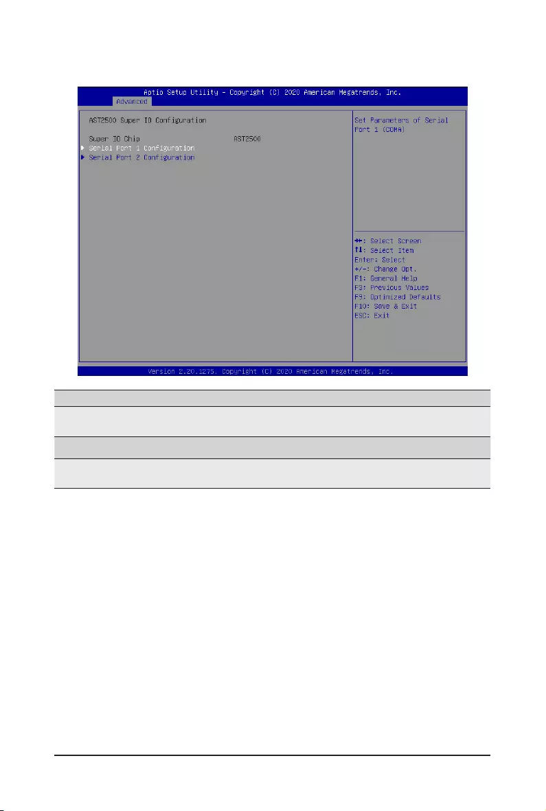
2-2-4 AST2500 Super IO Conguration
Parameter Description
AST2500 Super IO
Conguration
Super IO Chip Displays the super IO chip information
Serial Port 1/2
Conguration Press[Enter]forcongurationofadvanceditems.
BIOS Setup - 38 -
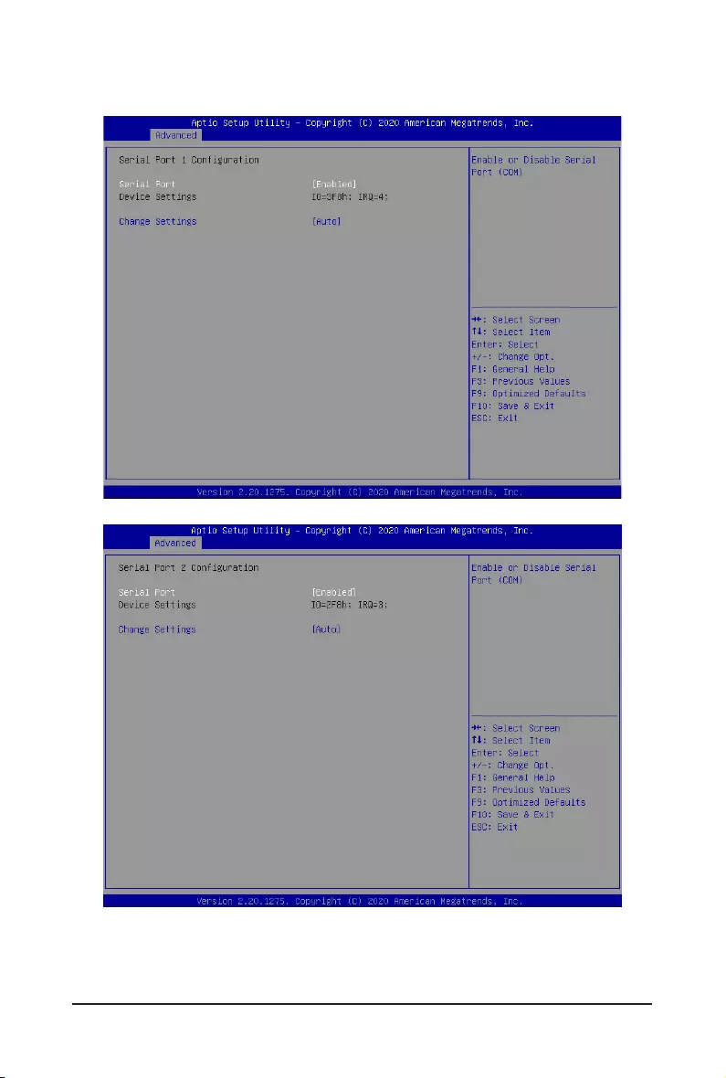
2-2-4-1 Serial Port 1/2 Conguration

- 39 - BIOS Setup
Parameter Description
SerialPort1/2Conguration
Serial Port(Note1)
Enable/Disable the Serial Port (COM). When set to Enabled allows you to
conguretheSerialport1/2settings.WhensettoDisabled,displaysno
congurationfortheserialport.
Options available: Enabled, Disabled. Default setting is Enabled.
Devices Settings(Note2) Displays the Serial Port 1/2 device settings.
Change Settings(Note2)
Select an optimal settings for Super IO Device.
Options available for Serial Port 1:
Auto
IO=3F8h; IRQ=4;
IO=3F8h; IRQ=3, 4, 5, 6, 7, 9, 10, 11, 12;
IO=2F8h; IRQ=3, 4, 5, 6, 7, 9, 10, 11, 12;
IO=3E8h; IRQ=3, 4, 5, 6, 7, 9, 10, 11, 12;
IO=2E8h; IRQ=3, 4, 5, 6, 7, 9, 10, 11, 12;
Default setting is Auto.
Options available for Serial Port 2:
Auto
IO=2F8h; IRQ=3;
IO=3F8h; IRQ=3, 4, 5, 6, 7, 9, 10, 11, 12;
IO=2F8h; IRQ=3, 4, 5, 6, 7, 9, 10, 11, 12;
IO=3E8h; IRQ=3, 4, 5, 6, 7, 9, 10, 11, 12;
IO=2E8h; IRQ=3, 4, 5, 6, 7, 9, 10, 11, 12;
Default setting is Auto.
Please note that this item is congurable when Serial Port is set to
Enabled.
(Note1) Advanceditemspromptwhenthisitemisdened.
(Note2) This item appears when Serial Port is set to Enabled.
BIOS Setup - 40 -
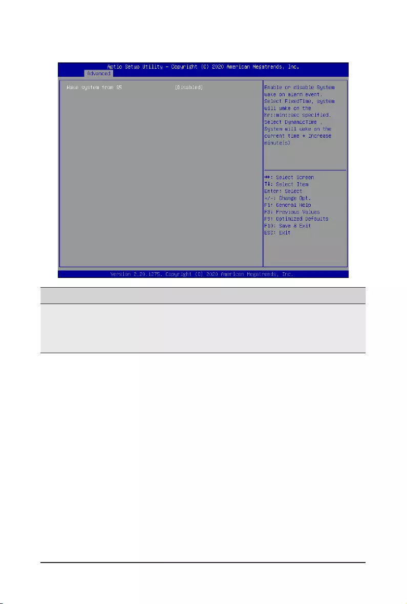
2-2-5 S5 RTC Wake Settings
Parameter Description
Wake System from S5
Enable/Disable system wake on alarm event.
Options available: Disabled, Fixed Time, Dynamic Time. When Fixed Time is
selected,systemwillwakeonthehr::min::secspecied.
Default setting is Disabled.
- 41 - BIOS Setup
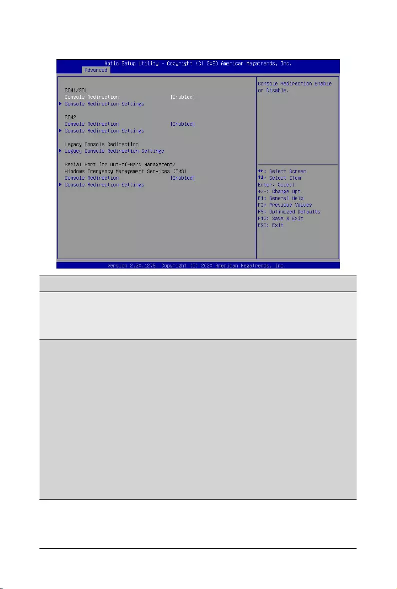
2-2-6 Serial Port Console Redirection
(Note) Advanceditemspromptwhenthisitemisdened.
Parameter Description
COM1/Serial Over
LAN & COM2 Console
Redirection(Note))
Selectwhethertoenableconsoleredirectionforspecieddevice.Console
redirection enables the users to manage the system from a remote
location.
Options available: Enabled, Disabled. Default setting is Disabled.
COM1/Serial Over LAN &
COM2 Console Redirection
Settings
Press[Enter]tocongureadvanceditems.
Please note that this item is congurable when COM1/Serial Over
LAN & COM2 Console Redirection is set to Enabled.
Terminal Type
– Selects a terminal type to be used for console redirection.
– Options available: VT100, VT100+, ANSI, VT-UTF8. Default setting
is ANSI.
Bits per second
– Selects the transfer rate for console redirection.
– Options available: 9600, 19200, 38400, 57600, 115200. Default
setting is 115200.
Data Bits
– Selects the number of data bits used for console redirection.
– Options available: 7, 8. Default setting is 8.

BIOS Setup - 42 -
(Note) Advanceditemspromptwhenthisitemisdened.
Parameter Description
COM1/Serial Over LAN &
COM2 Console Redirection
Settings (continued)
Parity
– A parity bit can be sent with the data bits to detect some
transmission errors.
– Even: parity bit is 0 if the num of 1's in the data bits is even.
– Odd: parity bit is 0 if num of 1's in the data bits is odd.
– Mark: parity bit is always 1. Space: Parity bit is always 0.
– Mark and Space Parity do not allow for error detection.
– Options available: None, Even, Odd, Mark, Space. Default setting
is None.
Stop Bits
– Stop bits indicate the end of a serial data packet. (A start bit
indicates the beginning). The standard setting is 1 stop bit.
Communication with slow devices may require more than 1 stop
bit.
– Options available: 1, 2. Default setting is 1.
Flow Control
– Flowcontrolcanpreventdatalossfrombufferoverow.When
sending data, if the receiving buffers are full, a 'stop' signal can
besenttostopthedataow.Oncethebuffersareempty,a'start'
signalcanbesenttore-starttheow.Hardwareowcontroluses
two wires to send start/stop signals.
– Options available: None, Hardware RTS/CTS. Default setting is
None.
VT-UTF8 Combo Key Support
– Enable/Disable the VT-UTF8 Combo Key Support.
– Options available: Enabled, Disabled. Default setting is Enabled.
Recorder Mode(Note)
– When this mode enabled, only texts will be send. This is to capture
Terminal data.
– Options available: Enabled, Disabled. Default setting is Disabled.
Resolution 100x31(Note)
– Enable/Disable extended terminal resolution.
– Options available: Enabled, Disabled. Default setting is Enabled.
Putty KeyPad(Note)
– Selects FunctionKey and LeyPad on Putty.
– Options available: VT100, LINUX, XTERMR6, SC0, ESCN, VT400.
Default setting is VT100.

- 43 - BIOS Setup
Parameter Description
Legacy Console Redirection
Legacy Console Redirection
Settings
Press[Enter]tocongureadvanceditems.
Redirection COM Port
– Selects a COM port for Legacy serial redirection.
– Options available: COM1/SOL, COM2. Default setting is COM1/
SOL.
Resolution
– Selects the number of rows and columns used in Console
Redirection for legacy OS support.
– Options available: 80x24, 80x25. Default setting is 80x24.
Redirect After POST
– When Bootloader is selected, then Legacy Console Redirection
is disabled before booting to legacy OS. When Always Enable is
selected, then Legacy Console Redirection is enabled for legacy
OS.
– Options available: Always Enable, BootLoader. Default setting is
Always Enable.
Serial Port for Out-of-Band
Management / Windows
Emergency Management
Services (EMS) Console
Redirection(Note)
EMSconsoleredirectionallowstheusertocongureConsoleRedirection
Settings to support Out-of-Band Serial Port management.
Options available: Enabled, Disabled. Default setting is Disabled.
Serial Port for Out-of-Band
EMS Console Redirection
Settings
Press[Enter]tocongureadvanceditems.
Please note that this item is congurable when Serial Port for Out-of-
Band Management EMS Console Redirection is set to Enabled.
Out-of-Band Mgmt Port
– Microsoft Windows Emerency Management Service (EMS) allows
for remote management of a Windows Server OS through a serial
port.
– Options available: COM1/SOL, COM2. Default setting is COM1/
SOL.
Terminal Type
– Selects a terminal type to be used for console redirection.
– Options available: VT100, VT100+, ANSI, VT-UTF8. Default setting
is ANSI.
Bits per second
– Selects the transfer rate for console redirection.
– Options available: 9600, 19200, 38400, 57600, 115200. Default
setting is 115200.
(Note) Advanceditemspromptwhenthisitemisdened.

BIOS Setup - 44 -
Parameter Description
Serial Port for Out-of-Band
EMS Console Redirection
Settings(continued)
Flow Control
– Flowcontrolcanpreventdatalossfrombufferoverow.When
sending data, if the receiving buffers are full, a 'stop' signal can
besenttostopthedataow.Oncethebuffersareempty,a'start'
signalcanbesenttore-starttheow.Hardwareowcontroluses
two wires to send start/stop signals.
– Options available: None, Hardware RTS/CTS, Software Xon/Xoff.
Default setting is None.
- 45 - BIOS Setup
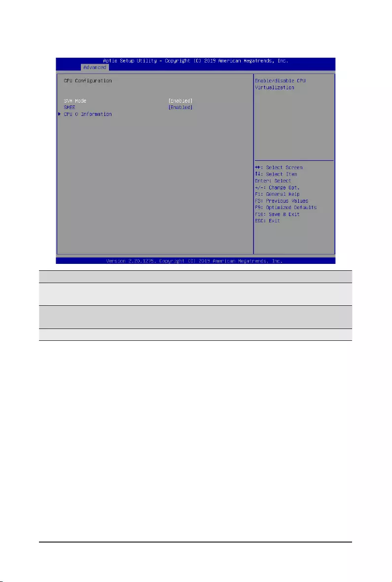
2-2-7 CPU Conguration
Parameter Description
SVM Mode Enable/Disable the CPU Virtualization.
Options available: Enabled, Disabled. Default setting is Enabled.
SMEE Controls the Secure Memory Encryption Enable (SMEE) function.
Options available: Enabled, Disabled. Default setting is Enabled.
CPU 0/1 Information Press [Enter] to view the memory information related to CPU 0/1.
BIOS Setup - 46 -
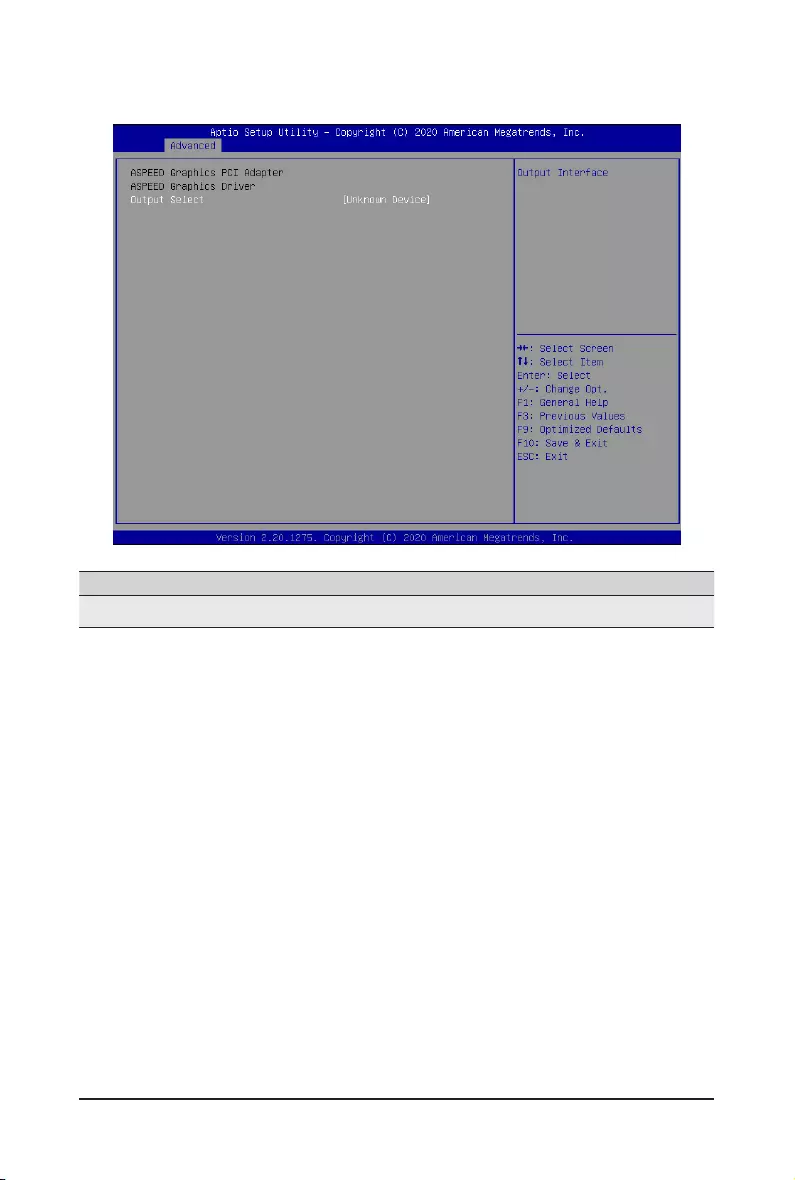
2-2-8 AMI Graphic Output Protocol Policy
Parameter Description
Output Select Selects Monitor Output by Graphic Output Protocol.
- 47 - BIOS Setup
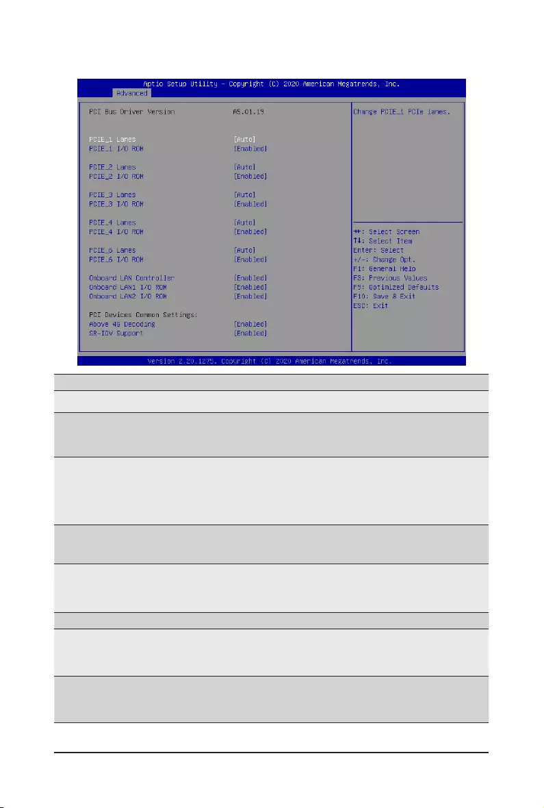
2-2-9 PCI Subsystem Settings
Parameter Description
PCI Bus Driver Version Displays the PCI Bus Driver version information.
PCIE_#(Note1) LanesConguration
Change the PCIe lanes.
Options available: Disabled, Auto, x8, x4x4, x16, x8x8, x8x4x4,
x4x4x8, x4x4x4x4. Default setting is Auto.
PCI Express Slot # I/O ROM (Note1)
When enabled, this setting will initialize the device expansion ROM
for the related PCI-E slot.
Options available: Enabled, Disabled. Default setting is Enabled.
Onboard LAN Controller(Note2) Enable/Disable the onboard LAN devices.
Options available: Enabled, Disabled. Default setting is Enabled.
Onboard LAN I/O ROM(Note2)
Enable/Disable the onboard LAN devices, and initializes device
expansion ROM.
Options available: Enabled, Disabled. Default setting is Enabled.
PCI Devices Common Settings
Above 4G Decoding
Enable/Disable memory mapped I/O to 4GB or greater address
space (Above 4G Decoding).
Options available: Enabled, Disabled. Default setting is Enabled.
SR-IOV Support
If the system has SR-IOV capable PCIe devices, this item Enable/
Disable Single Root IO Virtualization Support.
Options available: Enabled, Disabled. Default setting is Enabled.
(Note1) This section is dependent on the available PCIe Slot.
(Note2) This section is dependent on the available LAN controller.
BIOS Setup - 48 -
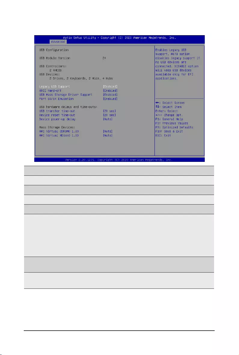
2-2-10 USB Conguration
(Note) This item is present only if you attach USB devices.
Parameter Description
USBConguration
USB Module Version Displays the USB module version information.
USB Controllers Displays the supported USB controllers.
USB Devices: Displays the USB devices connected to the system.
Legacy USB Support
Enable/Disable the Legacy USB support fuction. AUTO option
disables legacy support if no USB devices are connected.
DISABLE option will keep USB devices available only for EFI
applications.
Options available: Auto, Enabled, Disabled. Default setting is
Enabled.
XHCI Hand-off Enable/Disable the XHCI (USB 3.0) Hand-off support.
Options available: Enabled, Disabled. Default setting is Enabled.
USB Mass Storage Driver
Support(Note)
Enable/Disable the USB Mass Storage Driver Support.
Options available: Enabled, Disabled. Default setting is Enabled.

- 49 - BIOS Setup
Parameter Description
Port 60/64 Emulation
Enables the I/O port 60h/64h emulation support. This should be
enabled for the complete USB Keyboard Legacy support for non-
USB aware OS.
Options available: Enabled, Disabled. Default setting is Enabled.
USB hardware delays and time-outs
USB transfer time-out
Selects the time-out value for USB Control/Bulk/Interrupt transfers.
Options available: 1 sec, 5 sec, 10 sec, 20sec.
Default setting is 20 sec.
Device reset time-out
Selects the time-out value during a USB mass storage device
reset.
Options available: 10 sec, 20 sec, 30 sec, 40sec.
Default setting is 20 sec.
Device power-up delay
Maximum time the device will take before it properly reports itself
to the Host Controller. "Auto" uses default value: for a Root port it
is 100 ms, for a Hub port the delay is taken from Hub descriptor.
Options available: Auto, Manual. Default setting is Auto.
Mass Storage Devices Displays the mass storage devices avaiable on the system.
BIOS Setup - 50 -
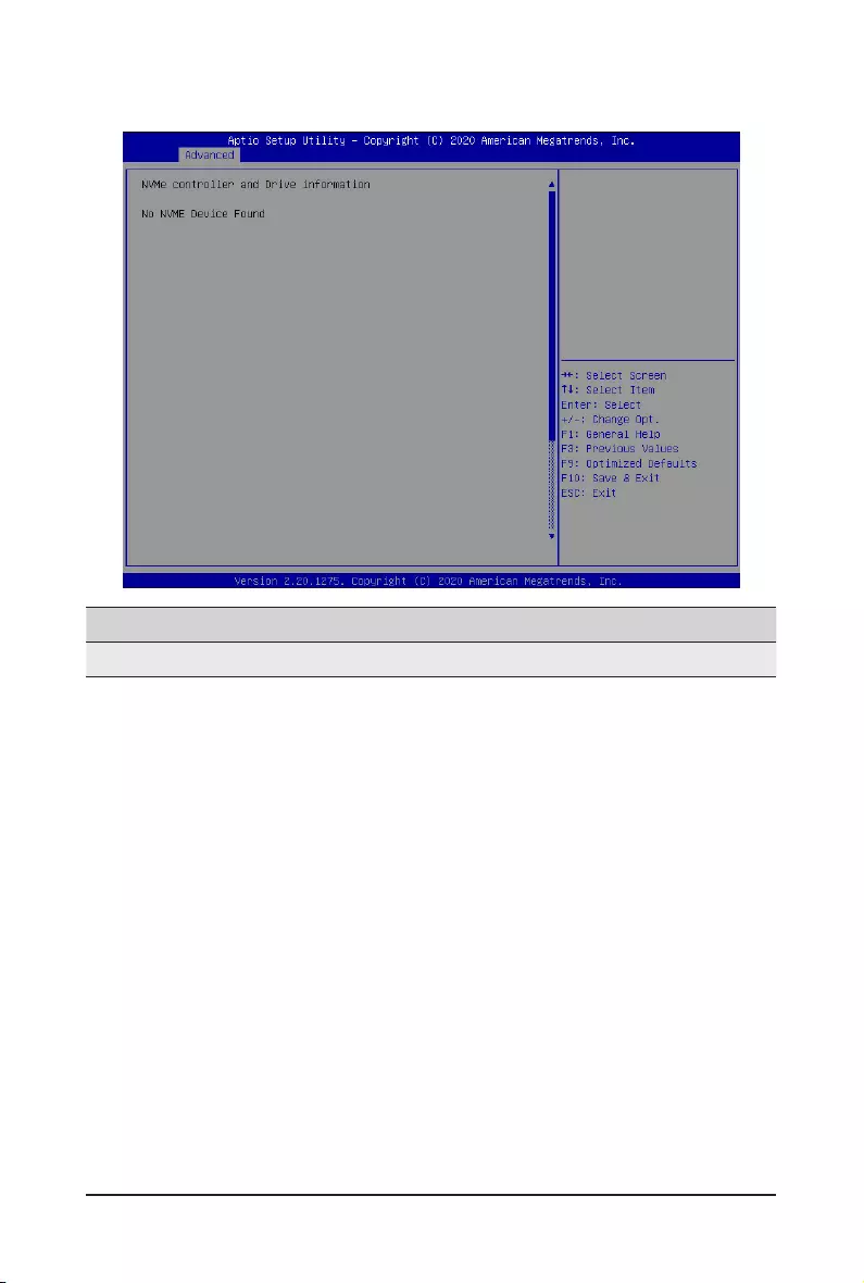
2-2-11 NVMe Conguration
Parameter Description
NVMeConguration Displays the NVMe devices connected to the system.
- 51 - BIOS Setup
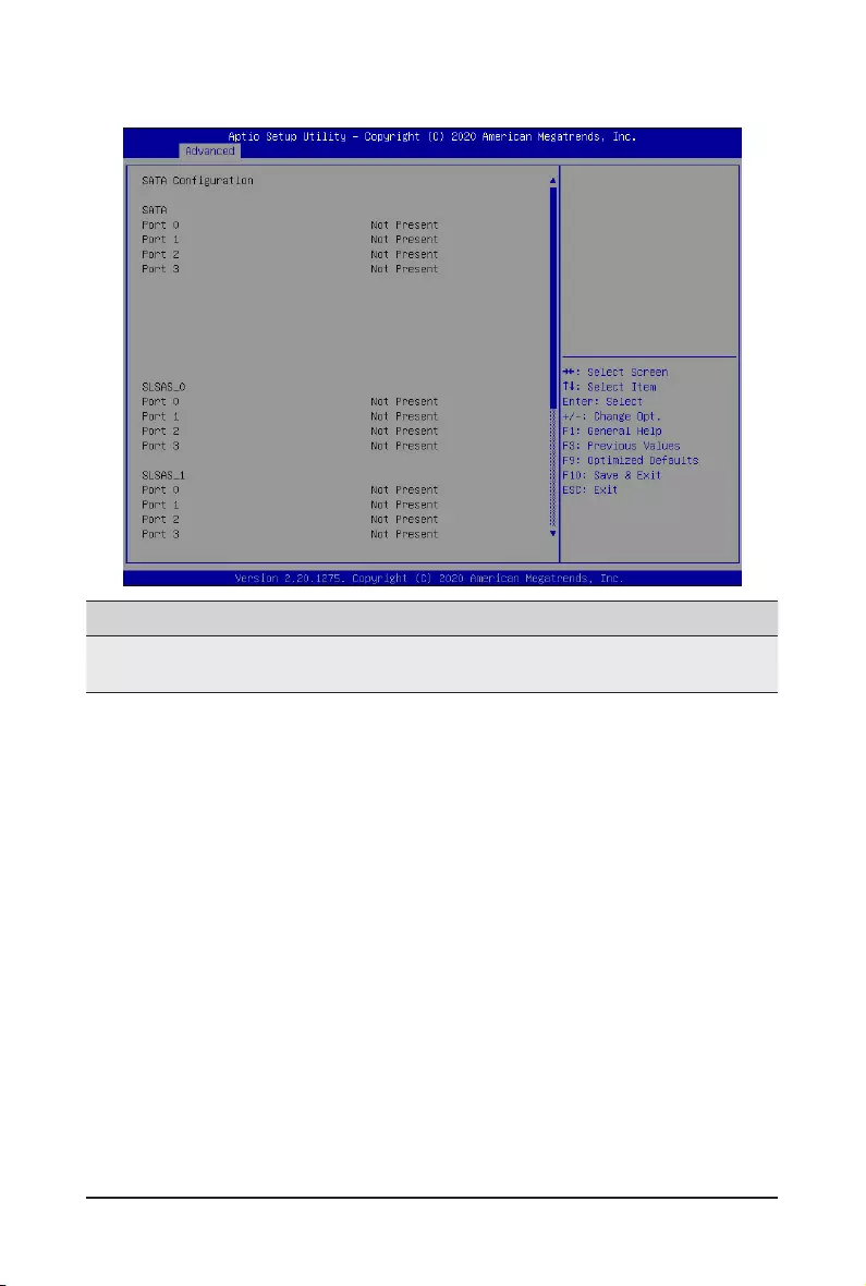
2-2-12 SATA Conguration
Parameter Description
SATAConguration Displays the installed HDD devices information. System will automatically
detect HDD type.
BIOS Setup - 52 -
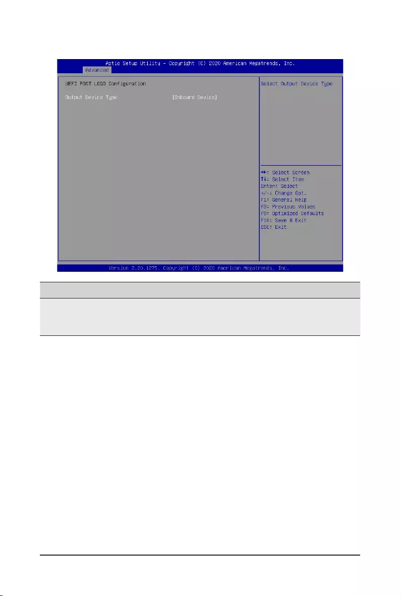
2-2-13 UEFI POST LOGO Conguration
Parameter Description
Output Device Type
Selects output device type.
Options available: First loaded Device, Onboard Device, External Device,
SpecicDevice.DefaultsettingisOnboard Device.
- 53 - BIOS Setup
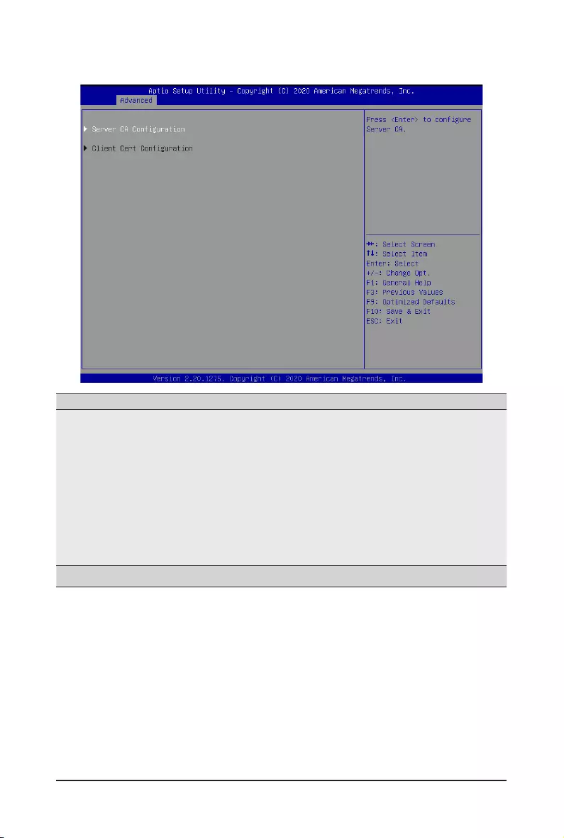
2-2-14 T1s Auth Conguration
Parameter Description
ServerCAConguration
Press[Enter]forcongurationofadvanceditems.
Enroll Cert
–Press[Enter]toenrollacerticate
• Enroll Cert Using File
• Cert GUID
Input digit character in 1111111-2222-3333-4444-1234567890ab
format.
– Commit Changes and Exit
– Discard Changes and Exit
Delete Cert
ClientCertConguration Press[Enter]forcongurationofadvanceditems.
BIOS Setup - 54 -
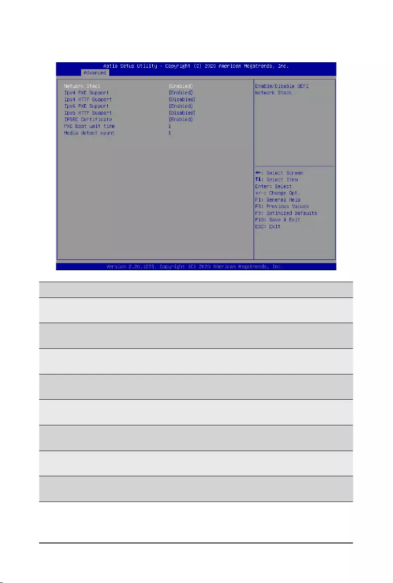
2-2-15 Network Stack Conguration
(Note) This item appears when Network Stack is set to Enabled.
Parameter Description
Network Stack Enable/Disable the UEFI network stack.
Options available: Enabled, Disabled. Default setting is Enabled.
Ipv4 PXE Support(Note) Enable/Disable the Ipv4 PXE feature.
Options available: Enabled, Disabled. Default setting is Enabled.
Ipv4 HTTP Support(Note) Enable/Disable the Ipv4 HTTP feature.
Options available: Enabled, Disabled. Default setting is Disabled.
Ipv6 PXE Support(Note) Enable/Disable the Ipv6 PXE feature.
Options available: Enabled, Disabled. Default setting is Enabled.
Ipv6 HTTP Support(Note) Enable/Disable the Ipv6 HTTP feature.
Options available: Enabled, Disabled. Default setting is Disabled.
IPSECCerticate(Note) Enable/DisabletheIPSECCerticatefeature.
Options available: Enabled, Disabled. Default setting is Enabled.
PXE boot wait time(Note) Wait time in seconds to press ESC key to abort the PXE boot.
Press the <+> / <-> keys to increase or decrease the desired values.
Media detect count(Note) Number of times the presence of media will be checked.
Press the <+> / <-> keys to increase or decrease the desired values.
- 55 - BIOS Setup
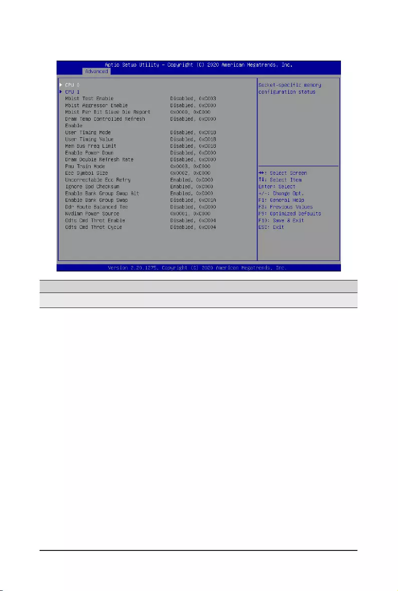
2-2-16 AMD Mem Conguration Status
Parameter Description
CPU0/1 Press[Enter]toviewthememorycongurationstatusrelatedtoCPU0/1.
BIOS Setup - 56 -
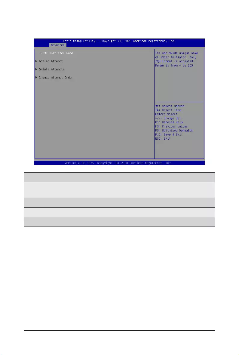
2-2-17 iSCSI Conguration
Parameter Description
iSCSI Initiator Name Press [Enter] and name iSCSI Initiator. Only IQN format is accecpted.
Range: from 4 to 223
Add an Attempt Press[Enter]tocongureadvanceditems.
Delete Attempts Press[Enter]tocongureadvanceditems.
Change Attempt Order Press[Enter]tocongureadvanceditems.
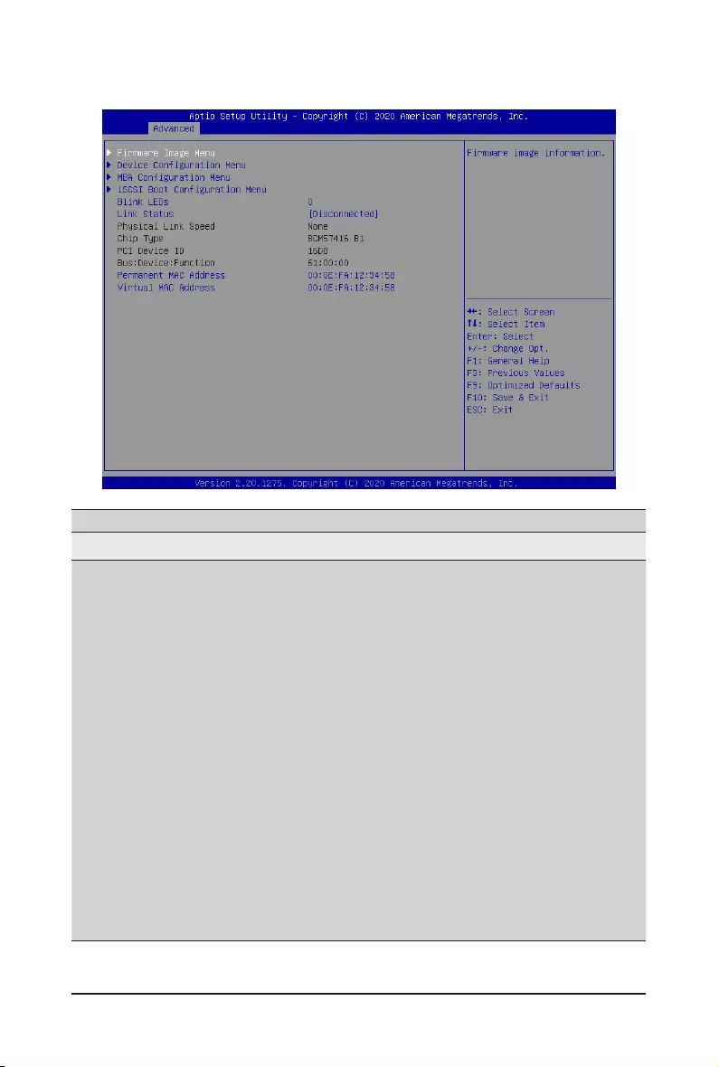
- 57 - BIOS Setup
2-2-18 Broadcom BCM57416 10GBASE-T Network Connection
Parameter Description
Firmware Image Menu Press[Enter]toviewrmwareimageinformation.
DeviceCongurationMenu
Press[Enter]tocongureadvanceditems.
Multi-Function Mode
– CongurestheNICHardwareMode.
– Options available: SF, NPAR 1.0. Default setting is SF.
Number of VFs Per PF
– ConguresthenumberofVirtualFunctionsPerPhysicalFunctionin
multiplesof8(1-128).ThiseldisonlyapplicablewhenSR-IOVis
enabled.
– Default setting is 8.
SR-IOV
– Enable/Disable Single Root I/O Virtualization.
– Options available: Enabled, Disabled. Default setting is Enabled.
Number of MSI-X Vectors per VF
– ConguresthenumberofMSI-XVectorsperVF(0-128).
– Default setting is 4.
Maximum Number of PF MSI-X Vectors
– ConguresthemaximumnumberofPFMSI-XVectors(0-512per
controller).
– Default setting is 74.

BIOS Setup - 58 -
Parameter Description
DeviceCongurationMenu
(continued)
EnergyEfcientEthernet
– Enable/DisableEnergyEfcientEthernetoperation.
– Options available: Enabled, Disabled. Default setting is Enabled.
Operational Link Speed
– Conguresthelinkspeedsettingtobeusedasthedefaultlinkspeed
for the selected port.
– Options available: AutoNeg. Default setting is AutoNeg.
Firmware Link Speed
– Conguresthelinkspeedsettingtobeusedasthedefaultlinkspeed
for selected port in D3 state.
– Options available: AutoNeg. Default setting is AutoNeg.
Support RDMA
– Enable/Disable RDMA support for this port.
– Options available: Enabled, Disabled. Default setting is Disabled.
DCB Protocol
– Enable/Disable DCB protocol.
– Options available: Disabled, Enabled (IEEE only), CEE (only), Both
(IEEE preferred with fallback to CEE). Default setting is Disabled.
LLDP nearest bridge
– Enable/Disable LLDP nearest bridge state.
– Options available: Enabled, Disabled. Default setting is Enabled.
LLDP nearest non-TPMR bridge
– Enable/Disable LLDP earest non-TPMR bridge state.
– Options available: Enabled, Disabled. Default setting is Enabled.
Default EVB Mode
– ConguresthedefaultEdgeVirtualBridgingmode.
– Options available: VEB, VEPA, None. Default setting is VEB.
Enable PME Capability
– Enable/Disable PME Capability support.
– Options available: Enabled, Disabled. Default setting is Disabled.
Open Virtual Switch
– Enable/Disable Open Virtual Switch.
– Options available: Enabled, Disabled. Default setting is Disabled.
MBACongurationMenu
Press[Enter]tocongureadvanceditems.
Option ROM
– Enable/Disable Boot Option ROM.
– Options available: Enabled, Disabled. Default setting is Enabled.
Legacy Boot Protocol
– Selects non-UEFI Boot Protocol: Preboot Execution Environment
(PXE)/iSCSI.
– Options available: PXE, iSCSI, NONE. Default setting is PXE.
Boot Strap Type
– Selects the boot strap type.Options available: Auto Detect, BBS, Int
18h, Int 19h. Default setting is Auto Detect.

BIOS Setup - 59 -
Parameter Description
MBACongurationMenu
(continued)
Hide Setup Prompt
– CongureswhethertheSetupPromptisdisplayedduringROM
initialization.
– Options available: Enabled, Disabled. Default setting is Disabled.
Setup Key Stroke
– Congureskeystrokestoinvokethecongurationmenu.
– Options available: Ctrl-S, Ctrl-B. Default setting is Ctrl-S.
Banner Message Timeout
– Selects the timeout value. (0 defaults to 4 seconds, 15 is no delay,
1-14 is timeout value in seconds)
– Default setting is 4.
Pre-boot Wake On LAN
– ConguresPre-bootWakeonLAN(WOL).
– Options available: Enabled, Disabled. Default setting is Disabled.
VLAN Mode
– ConguresthevirtualLAN(VLAN)mode.
– Options available: Enabled, Disabled. Default setting is Disabled.
VLAN ID
– CongurestheVLANID(1…4094).
– This item is available only when VLAN Mode is Enabled.
Boot Retry Count
– Selects the number of boot retries.
– Options available: No Retry, 1 Retry, 2 Retries, 3 Retries, 4 Retries,
5Retries,6Retries,IndeniteRetries.DefaultsettingisNo Retry.
iSCSIBootConguration
Menu
Press[Enter]tocongureadvanceditems.
Blink LEDs IdentiesthephysicalnetworkportbyblinkingtheassociatedLED.
Pressthenumerickeystoadjustdesiredvalues.
Link Status Speciesthelinkstatusoftheport.
Physical Link Speed DisplaysthetechnicalspecicationsfortheNetworkInterfaceController.
Chip Type DisplaysthetechnicalspecicationsfortheNetworkInterfaceController.
PCI Device ID DisplaysthetechnicalspecicationsfortheNetworkInterfaceController.
Bus:Device:Function DisplaysthetechnicalspecicationsfortheNetworkInterfaceController.
Permanent MAC Address Displays the MAC address of the Ethernet controller.
Virtual MAC Address Displays the virtual MAC address of the Ethernet controller.
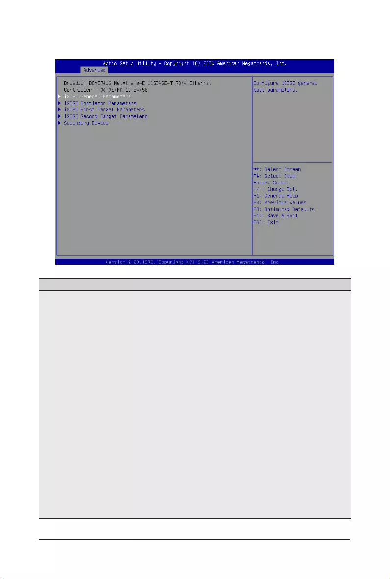
BIOS Setup - 60 -
2-2-18-1 iSCSI Boot Conguration Menu
Parameter Description
iSCSI General Parameters
Press[Enter]tocongureadvanceditems.
TCP/IP Parameters via DHCP
– Acquires TCP/IP Parameters via DHCP.
– Options available: Enabled, Disabled. Default setting is Enabled.
IPAutoconguration
– Auto-congurestheIPconguration.
– Options available: Enabled, Disabled. Default setting is Enabled.
– ThisitemiscongurablewhenTCP/IPParametersviaDHCPisset
to Disabled.
iSCSI Parameters via DHCP
– Acquires iSCSI Parameters via DHCP.
– Options available: Enabled, Disabled. Default setting is Disabled.
CHAP Authentication
– Enable/Disable the CHAP authentication.
– Options available: Enabled, Disabled. Default setting is Disabled.
Boot to iSCSI Target
– Enable/Disable booting to iSCSI target after log-on.
– Options available: Enabled, Disabled, One Time Disabled. Default
setting is Enabled.
DHCP Vendor ID
– CongurestheDHCPvendorID(upto32characterslong).

BIOS Setup - 61 -
Parameter Description
iSCSI General Parameters
(continued)
DHCP Vendor ID
– Conguresthelinkupdelaytimeinseconds(0-225).
Use TCP Timestamp
– Enable/Disable the TCP timestamp.
– Options available: Enabled, Disabled. Default setting is Disabled.
Target as First HDD
– Enable/Disabletargetappearsasrstharddiskdrive(HDD)inthe
system.
– Options available: Enabled, Disabled. Default setting is Disabled.
LUN Busy Retry Count
– Conguresthenumberofretriesin2secondintervalswhenLUNis
busy (0-60).
– Default setting is 0.
IP Version
– Displays the IP version supported. Modifying this parameter will reset
allIP-relatedelds.
– Options available: IPv4, IPv6. Disabled. Default setting is IPv4.
iSCSI Initiator Parameters
Press[Enter]tocongureadvanceditems.
IP Address
– CongurestheinitiatorIPaddress.
Subnet Mask
– CongurestheIPsubnetmask.
Default Gateway
– ConguresthedefaultgatewayIPaddress.
Primary DNS
– CongurestheprimaryDNSIPaddress.
Secondary DNS
– ConguresthesecondaryDNSIPaddress.
iSCSI Name
– CongurestheiSCSIname.
CHAP ID
– CongurestheChallenge-HandshakeAuthenticationProtocol
(CHAP) ID (up to 128 characters in length).
CHAP Secret
– ConguretheChallenge-HandshakeAuthenticationProtocol
(CHAP) Secret (12 to 16 characters in length).
iSCSI First/Second Target
Parameters
Press[Enter]tocongureadvanceditems.
Connect
– Enable/Disable the target establishment.
– Options available: Enabled, Disabled. Default setting is Disabled.
IP Address
– CongurestheTargetIPaddress.
TCP Port
– CongurestheTargetTCPportnumber(1-65535).

BIOS Setup - 62 -
Parameter Description
iSCSI First/Second Target
Parameters (continued)
TCP Port
– CongurestheTargetTCPportnumber(1-65535).
Boot LUN
– CongurestheTargetbootLUNnumber(0-255).
iSCSI Name
– CongurestheiSCSIname.
CHAP ID
– CongurestheChallenge-HandshakeAuthenticationProtocol
(CHAP) ID (up to 128 characters in length).
CHAP Secret
– ConguretheChallenge-HandshakeAuthenticationProtocol
(CHAP) Secret (12 to 16 characters in length).
Secondary Device
Press[Enter]tocongureadvanceditems.
Secondary Device
– Inputs the secondary device MAC addrss.
Use Independent Target Portal
– Use Independent target portal when multipath I/O is enabled.
– Options available: Enabled, Disabled. Default setting is Disabled.
Use Independent Target Name
– Use Independent target name when multipath I/O is enabled.
– Options available: Enabled, Disabled. Default setting is Disabled.
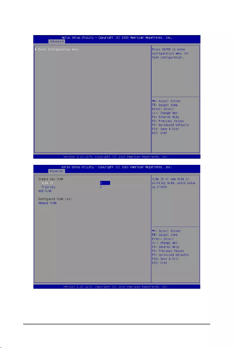
- 63 - BIOS Setup
2-2-19 VLAN Conguration

BIOS Setup - 64 -
Parameter Description
EnterCongurationMenu
Press[Enter]tocongureadvanceditems.
Create new VLAN
VLAN ID
– Sets VLAN ID for a new VLAN or an existing VLAN.
– Press the <+> / <-> keys to increase or decrease the desired values.
– The valid range is from 0 to 4094.
Priority
– Sets 802.1Q Priority for a new VLAN or an existing VLAN.
– Press the <+> / <-> keys to increase or decrease the desired values.
– The valid range is from 0 to 7.
Add VLAN
– Press [Enter] to create a new VLAN or update an existing VLAN.
ConguredVLANList
Remove VLAN
– Press [Enter] to remove an existing VLAN.
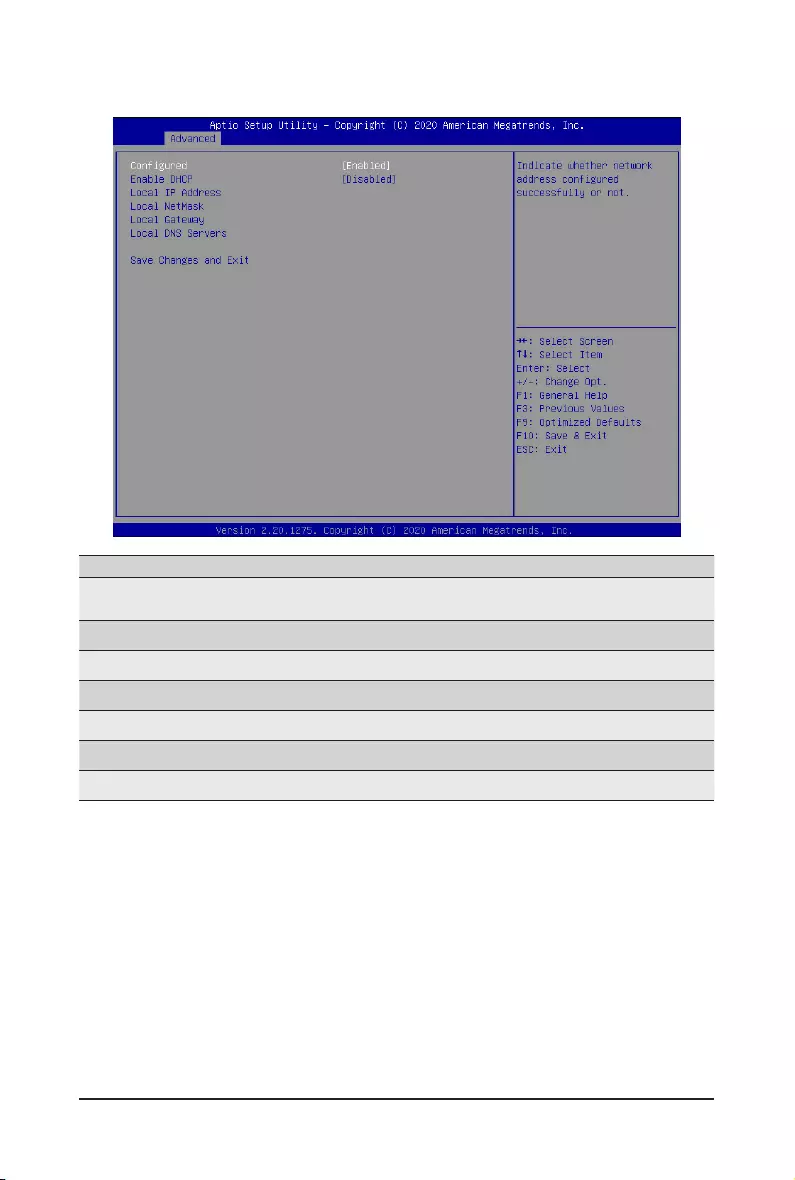
- 65 - BIOS Setup
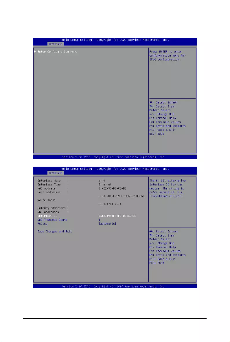
2-2-20 MAC IPv4 Network Conguration
Parameter Description
Congured Indicateswhethernetworkaddressisconguredsuccessfullyornot.
Options available: Enabled, Disabled. Default setting is Disabled.
Enable DHCP(Note) Options available: Enabled, Disabled. Default setting is Enabled.
Local IP Address(Note) Press[Enter]tocongurelocalIPaddress.
Local NetMask(Note) Press[Enter]tocongurelocalNetMask.
Local Gateway(Note) Press[Enter]tocongurelocalGateway
Local DNS Servers(Note) Press[Enter]tocongurelocalDNSservers
Save Changes and Exit Press[Enter]tosaveallcongurations.
(Note) This item appears when Congured is set to Enabled.
BIOS Setup - 66 -
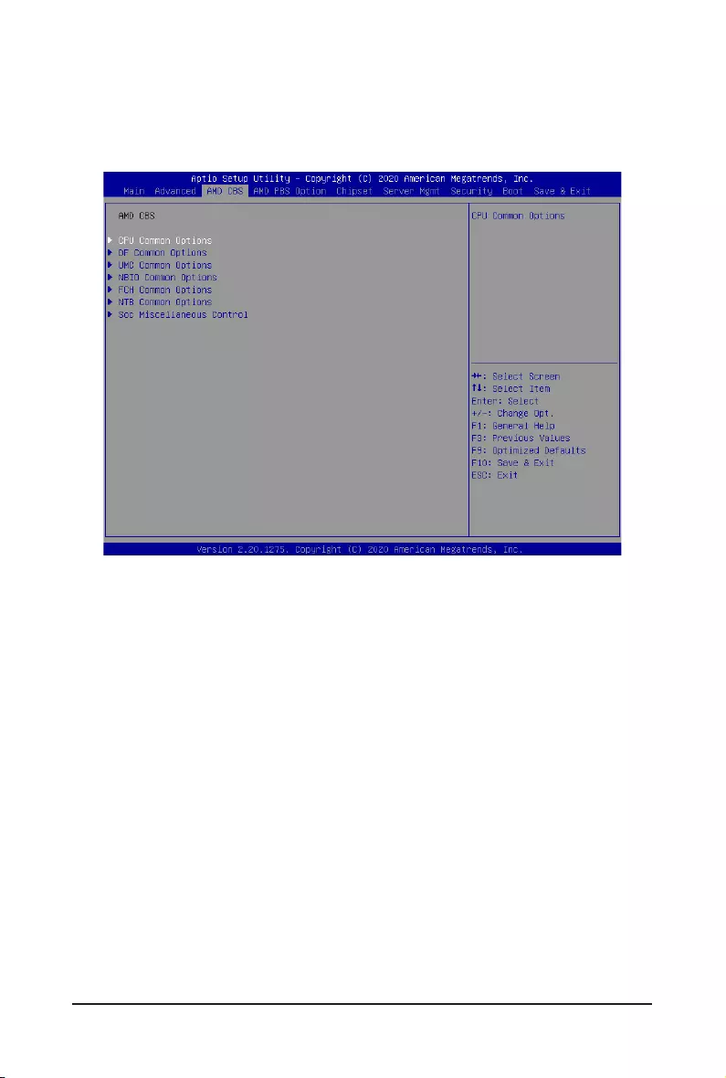
2-2-21 MAC IPv6 Network Conguration

- 67 - BIOS Setup
Parameter Description
EnterCongurationMenu
Press[Enter]tocongureadvanceditems.
Displays the MAC Address information.
Interface ID
– The 64 bit alternative interface ID for the device. The string is colon
separated. e.g. ff:dd:88:66:cc:1:2:3.
DAD Transmit Count
– The number of consective Neighbor solicitation messages sent while
performing Duplicate Address Detection on a tentative address.
A value of zero indicates that Duplicate Address Detection is not
performed.
Policy
– Options available: automatic, manual. Default setting is automatic.
Save Changes and Exit
– Press[Enter]tosaveallcongurations.
BIOS Setup - 68 -
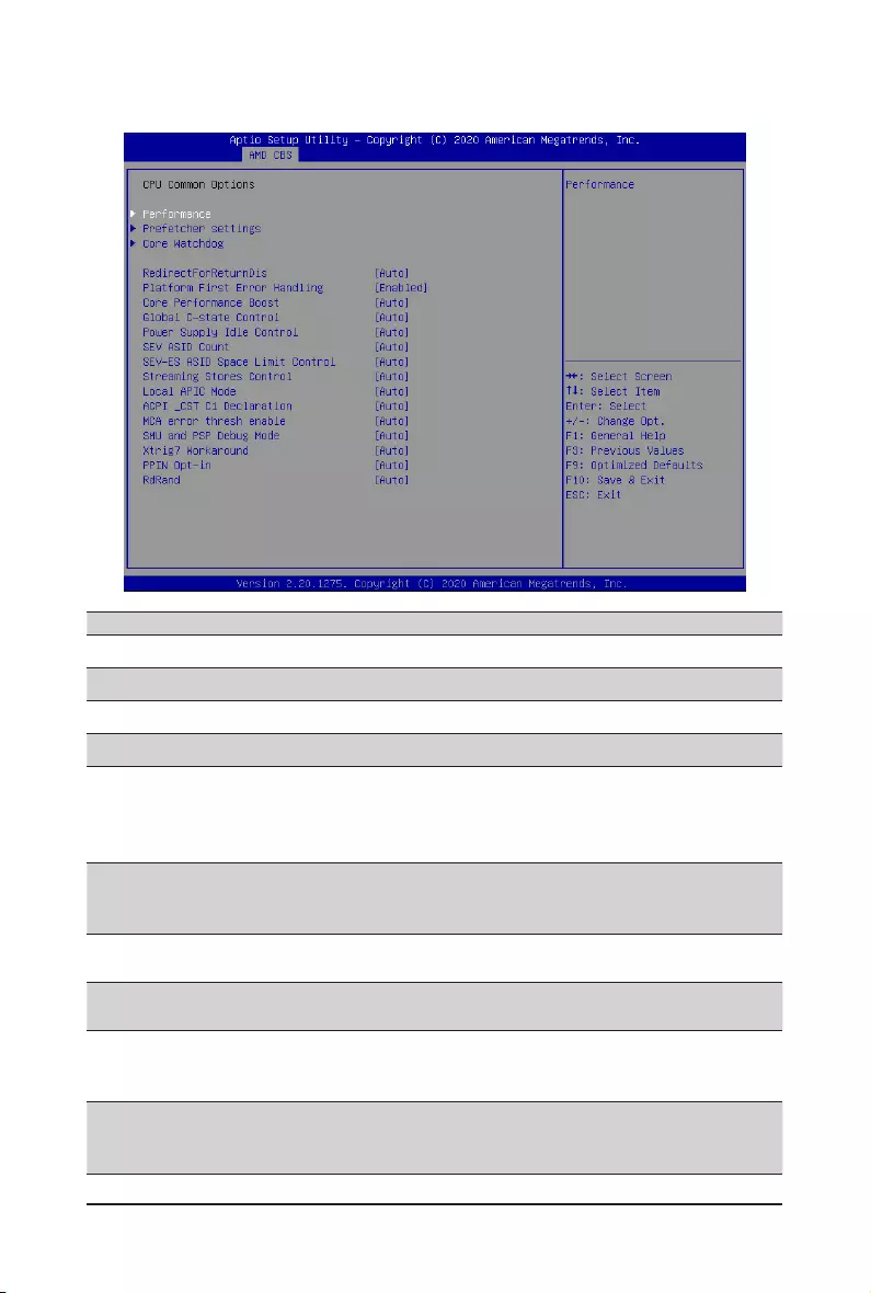
2-3 AMD CBS Menu
AMD CBS menu displays submenu options for configuring the CPU-related information that the BIOS
automatically sets. Select a submenu item, then press [Enter] to access the related submenu screen.
- 69 - BIOS Setup
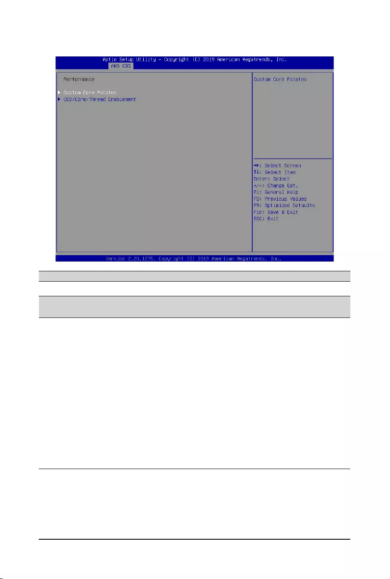
2-3-1 CPU Common Options
Parameter Description
CPU Common Options
Performance Press[Enter]forcongurationofadvanceditems.
Prefetcher settings Press[Enter]forcongurationofadvanceditems.
Core Watchdog Press[Enter]forcongurationofadvanceditems.
RedirectForReturnDis
From a workaround for GCC/C000005 issue for XV Core on CZ A0,
settingMSRC001_1029DecodeConguration(DE_CFG)bit14
[DecfgNoRdrctForReturns] to 1.
Options available: Auto, 1, 0. Default setting is Auto.
Platform First Error Handling
Enable/Disable PFEH, cloak individual banks, and mask deferred error
interrupts from each bank.
Options available: Auto, Enabled, Disabled. Default setting is Auto.
Core Performance Boost Enable/Disable the Core Performance Boost function.
Options available: Auto, Disabled. Default setting is Auto.
Global C-State Control Controls the IO based C-state generation and DF C-states.
Options available: Auto, Enabled, Disabled. Default setting is Auto.
Power Supply Idle Control
ConguresthePowerSupplyIdleControl.
Options available: Auto, Low Current Idle, Typical Current Idle. Default
setting is Auto.
SEV ASID Count
SpeciesthemaximumvalidASID,whichaffectsthemaximumsystem
physical address space.
Options available: Auto, 253 ASIDs, 509 ASIDs. Default setting is Auto.

BIOS Setup - 70 -
Parameter Description
SEV-ES ASID Space Limit
Control
Space limit control for SEV-ES ASIDs.
Options available: Auto, Manual. Default setting is Auto.
Streaming Stores Control Enable/Disable the Streaming Stores functionality.
Options available: Auto, Enabled, Disabled. Default setting is Auto.
Local APIC Mode Sets the Local APIC Mode.
Options available: Auto, xAPIC, x2APIC. Default setting is Auto.
ACPI_CST C1 Decaration Determines whether or not to declare the C1 state to the OS..
Options available: Auto, Enabled, Disabled. Default setting is Auto.
MCA error thresh enable Enable MCA error thresholding.
Options available: Auto, False, True. Default setting is Auto.
SMU and PSP Debug Mode
Whenthisoptionisenabled,specicuncorrectederrorsdetectedbythe
PSP FW or SMU FW will hand and not reset the system.
Options available: Auto, Enabled, Disabled. Default setting is Auto.
Xtrig7 Workaround Options available: Auto, No Workaround, Bronze Workaround, Sliver
Workaround. Default setting is Auto.
PPIN Opt-in Enable/Disable the PPIN feature.
Options available: Auto, Enabled, Disabled. Default setting is Auto.
- 71 - BIOS Setup
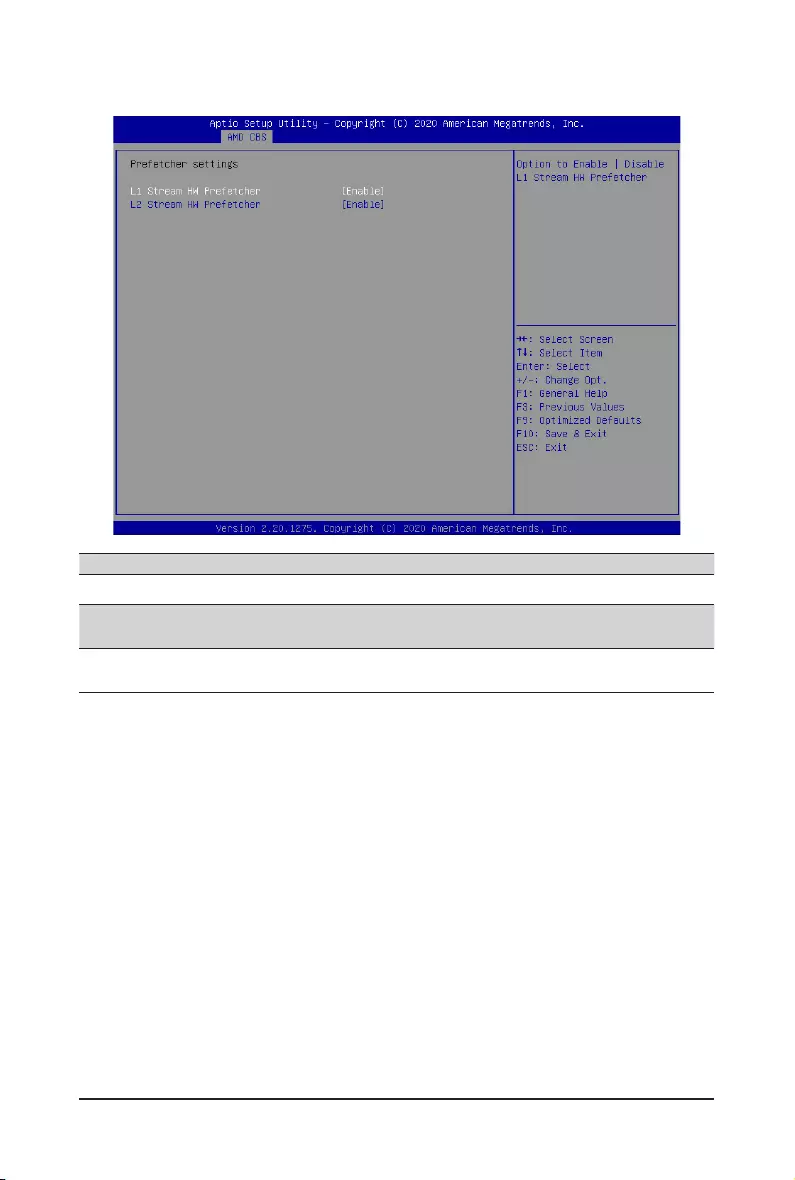
2-3-1-1 Performance
Parameter Description
Performance
Custom Core Pstates Allows you to accept or decline enabling Custom Core Pstates. When
accepted, you can disable or customize core pstates.
CCD/Core/Thread Enablement
Allows you to accept or decline enabling CCDs, processor cores and
threads. When accepted, you can control the number of CCDs to be
used, the number of cores to be used, and whether to enable or disable
Symmetric Multithreading Technology (SMT) support.
CCD Control
– Options available: Auto, 2 CCDs, 3CCDs, 4CCDs, 6CCDs. Default
setting is Auto.
Core Control
– Options available: Auto, TWO(1+1), FOUR(2+2), SIX(3+3). Default
setting is Auto.
SMT Control
– Disable: Single hardware thread per core.
– Auto: Two hardware threads per core.
– Options available: Disable, Auto. Default setting is Auto.
BIOS Setup - 72 -
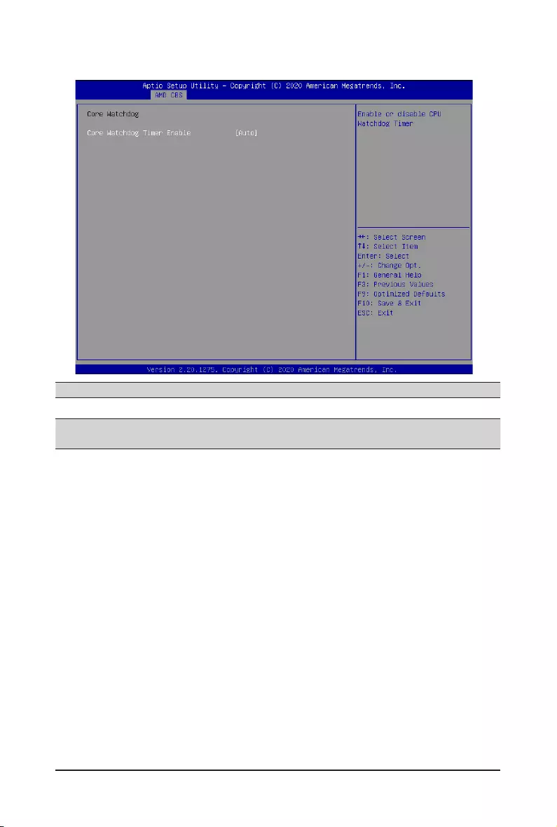
2-3-1-2 Prefetcher Settings
Parameter Description
Prefetcher settings
L1 Stream HW Prefetcher Enable/Disable L1 Stream HW Prefetcher.
Options available: Auto, Enabled, Disabled. Default setting is Auto.
L2 Stream HW Prefetcher Enable/Disable L2 Stream HW Prefetcher.
Options available: Auto, Enabled, Disabled. Default setting is Auto.
- 73 - BIOS Setup
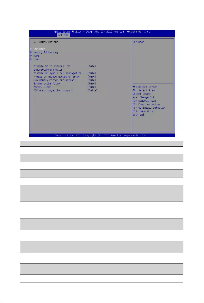
2-3-1-3 Core Watchdog
Parameter Description
Core Watchdog
Core Watchdog Timer Enable Enable/Disable CPU Watchdog Timer.
Options available: Auto, Enabled, Disabled. Default setting is Auto.
BIOS Setup - 74 -
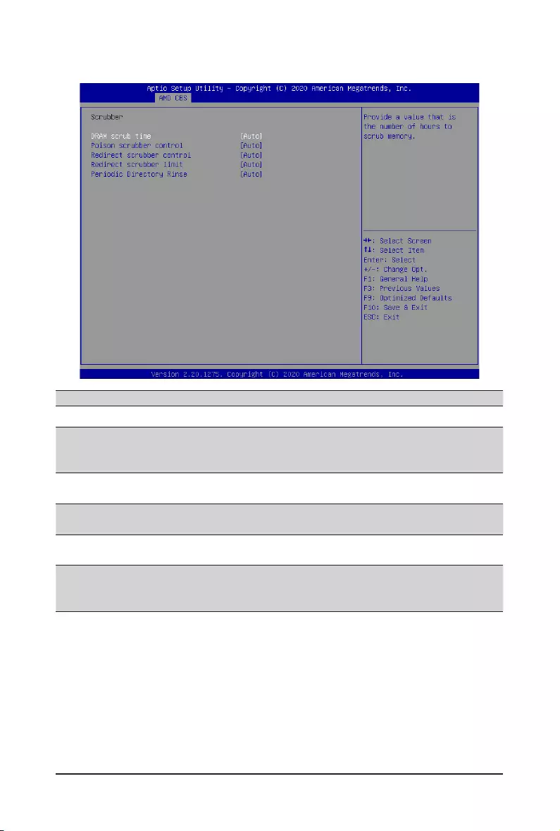
2-3-2 DF Common Options
Parameter Description
DF Common Options
Scrubber Press[Enter]forcongurationofadvanceditems.
Memory Addrssing Press[Enter]forcongurationofadvanceditems.
ACPI Press[Enter]forcongurationofadvanceditems.
Link Press[Enter]forcongurationofadvanceditems.
Disable DF to external IP
syncoodpropagation
Enable/Disable SyncFlood to UMC & downstream slaves.
Optionsavailable:Auto,Syncooddisabled,Syncoodenabled.
Default setting is Auto.
DisableDFsyncood
propagation
Enable/Disable DF Sync Flood propagation.
Optionsavailable:Auto,Syncooddisabled,Syncoodenabled.
Default setting is Auto.
Frezze DF module queues on
error Options available: Auto, Enabled, Disabled. Default setting is Auto.
CC6 memory region encryption Controls whether or not the CC6 save/restor memory is encrypted.
Options available: Auto, Enabled, Disabled. Default setting is Auto.
Systemprobelter Enable/DisableSystmeprobelter.
Options available: Auto, Enabled, Disabled. Default setting is Auto.
Memory Clear Enable/Disable the Memory Clear feature.
Options available: Auto, Enabled, Disabled. Default setting is Auto.
PSPerrorinjectionsupport Enable/DisablePSPerrorinjectionsupport.
Options available: False, True. Default setting is False.
- 75 - BIOS Setup
2-3-2-1 Scrubber
Parameter Description
Scrubber
DRAM scrub time
Provide a value that is the number of hours to scrub memory.
Options available: Auto, Disabled, 1 hour, 4 hours, 8 hours, 16 hours, 24
hours, 48 hours. Default setting is Auto.
Poison scrubber control Enable/Disable the Poison scrubber control feature.
Options available: Auto, Enabled, Disabled. Default setting is Auto.
Redirect scrubber control Enable/Disable the Redirect scrubber control feature.
Options available: Auto, Enabled, Disabled. Default setting is Auto.
Redirect scrubber limit Sets the redirect scrubber limit.
Optionsavailable:Auto,2,4,8,Innite.DefaultsettingisAuto.
Periodic Directory Rinse
Enable/Disable the Periodic Directory Rinse mode which may help manage
directorycapacitymoreefciently.
Options available: Auto, Enabled, Disabled. Default setting is Auto.
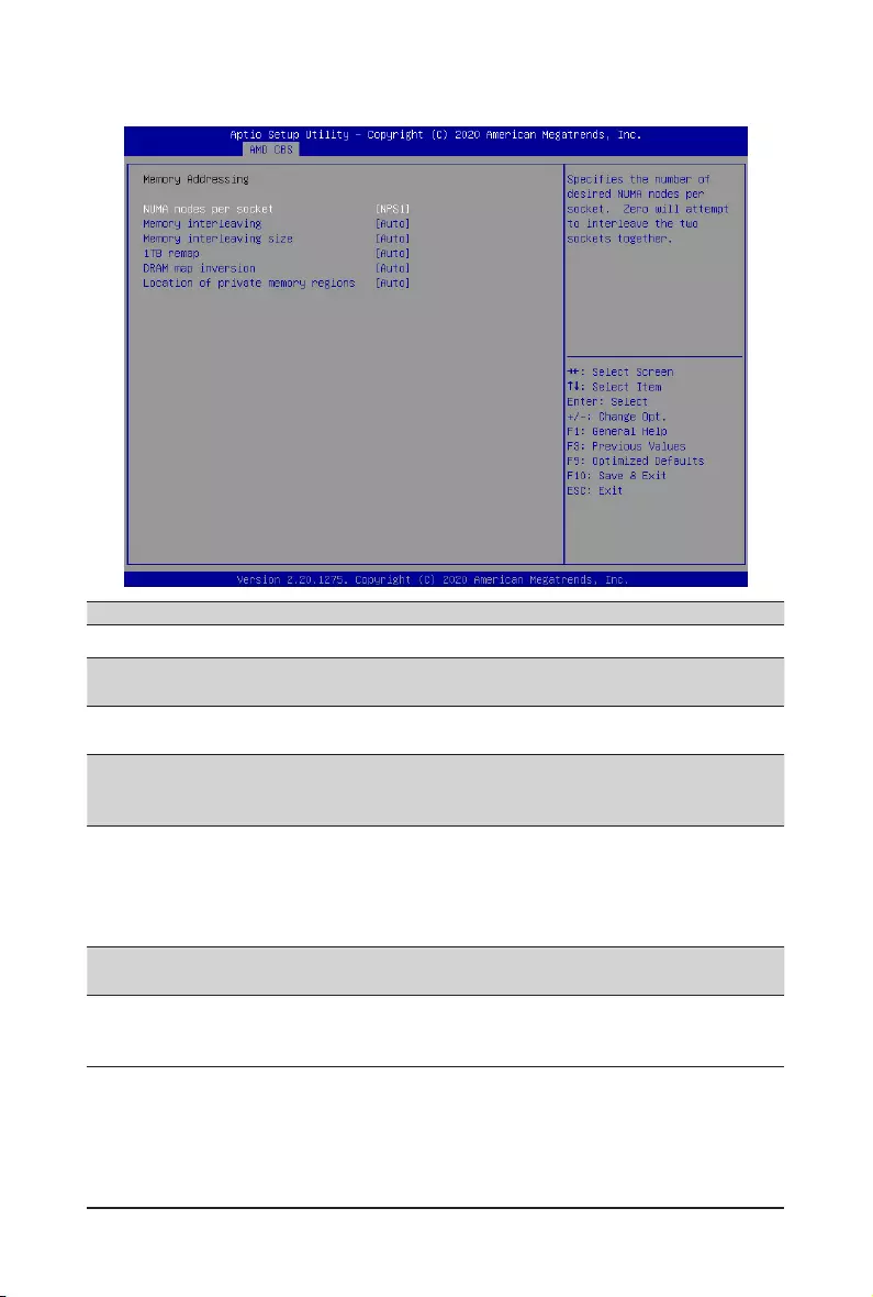
BIOS Setup - 76 -
2-3-2-2 Memory Addressing
Parameter Description
Memory Addressing
NUMA nodes per socket SpeciesthenumberofdesiredNUMAnodespersocket.
Options available: Auto, NPS0, NPS1, NPS2, NPS4. Default setting is Auto.
Memory inerleaving Enable/Disable the Memory interleaving feature.
Options available: Auto, Disabled. Default setting is Auto.
Memory interleaving size
Controls the memory interleaving size. This determines the starting address of
the interleave (bit 8, 9, 10 or 11).
Options available: Auto, 256Bytes, 512Bytes, 1KB, 2KB. Default setting is Auto.
1TB remap
Enable/DisabletoremapDRAMoutofthespacejustbelowthe1TBboundary.
TheabilitytoremapdependsonDRAMconguration,NPS,andinterleaving
selection, and may not always be possible.
Options available: Auto, Do not remap, Attempt to remap.
Default setting is Auto.
DRAM map inversion Enable/Disable the DRAM map inversion function.
Options available: Auto, Enabled, Disabled. Default setting is Auto.
Location of private memory
regions
Controls whether or not the private memory regions (PSP, SMU and CC6) are
at the top of DRAM or distributed.
Options available: Auto, Distributed, Consolidated. Default setting is Auto.
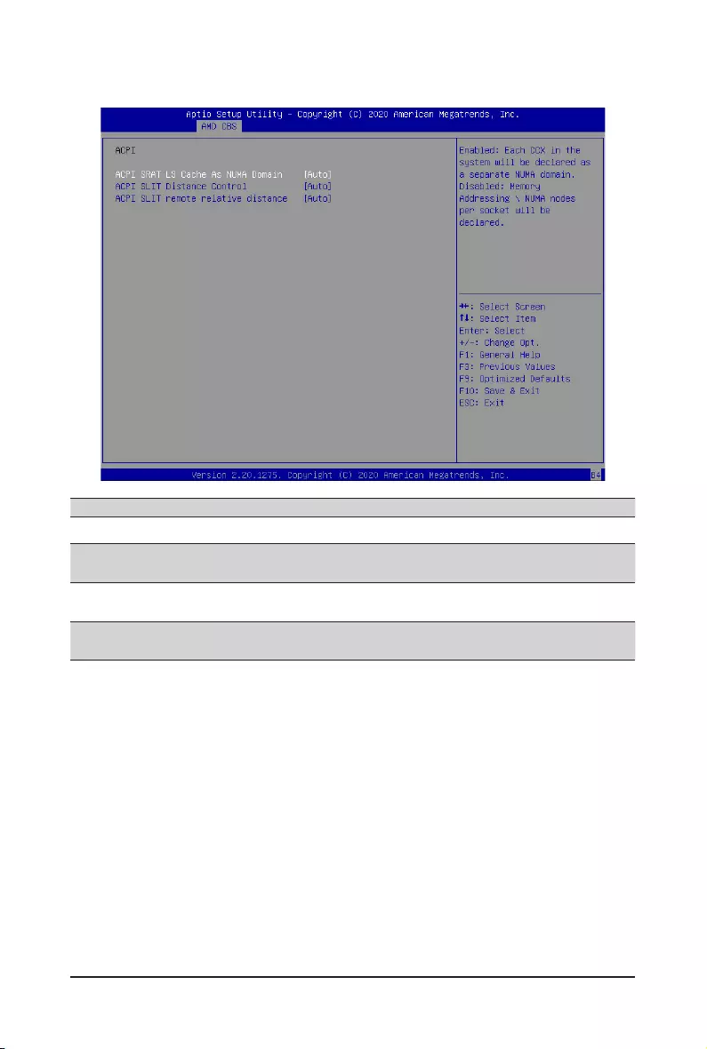
- 77 - BIOS Setup
2-3-2-3 ACPI
Parameter Description
ACPI
ACPI SRAT L3 Cache As
NUMA Domain
Enable/Disable report each L3 cache as a NUMA Domain to the OS.
Options available: Auto, Enabled, Disabled. Default setting is Auto.
ACPI SLIT Distance Control Determines how the SLIT distances are declared.
Options available: Auto, Manual. Default setting is Auto.
ACPI SLIT remote relative
distance
Sets the remote socket distance for 2P systems as near (2.8) or far (3.2).
Options available: Auto, Near, Far. Default setting is Auto.
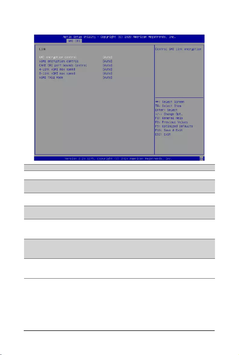
BIOS Setup - 78 -
2-3-2-4 Link
Parameter Description
Link
GMI encryption control Enable/Disable GMI link encryption.
Options available: Auto, Enabled, Disabled. Default setting is Auto.
xGMI encryption control Enable/Disable xGMI link encryption.
Options available: Auto, Enabled, Disabled. Default setting is Auto.
CAKE CRC perf bounds
Control Options available: Auto, Manual. Default setting is Auto.
4-link xGMI max speed
Speciesthemaxspeedof4-linkxGMI.
Options available: Auto, 10.667Gbps, 13Gbps, 16Gbps, 18Gbps.
Default setting is 10.667Gbps.
3-link xGMI max speed
Speciesthemaxspeedof3-linkxGMI.
Options available: Auto, 10.667Gbps, 13Gbps, 16Gbps, 18Gbps.
Default setting is 10.667Gbps.
xGMI TXEQ Mode
ConguresxGMITXEQ/RXvettingMode.
Options available: Auto, TXEQ_Disabled, TXEQ_Lane, TXEQ_Link,
TXEQ_RX_Vet. Default setting is 10.667Gbps.
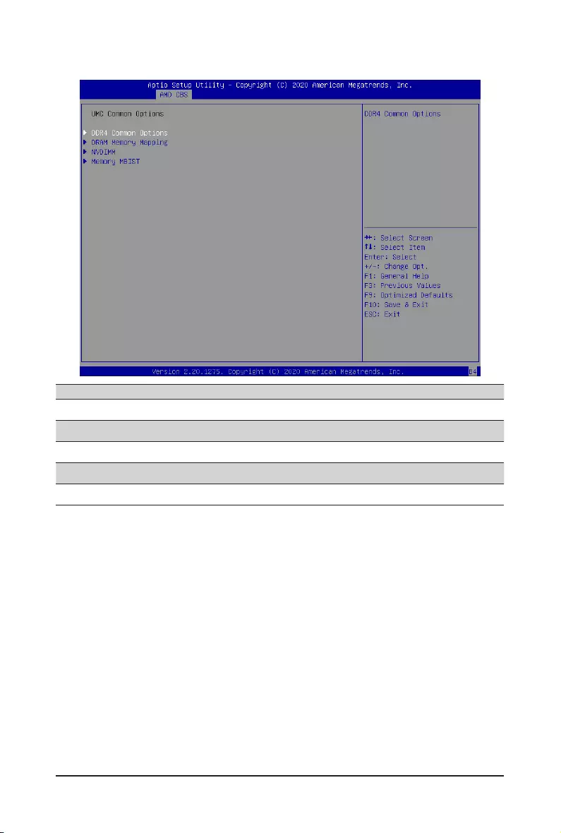
- 79 - BIOS Setup
2-3-3 UMC Common Options
Parameter Description
UMC Common Options
DDR4 Common Options Press[Enter]forcongurationofadvanceditems.
DRAM Memory Mapping Press[Enter]forcongurationofadvanceditems.
NVDIMM Press[Enter]forcongurationofadvanceditems.
Memory MBIST Press[Enter]forcongurationofadvanceditems.
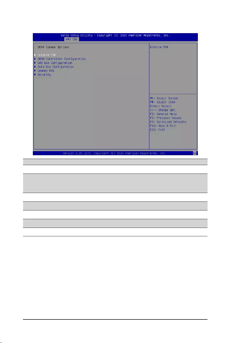
BIOS Setup - 80 -
2-3-3-1 DDR4 Common Options
Parameter Description
DDR4 Common Options
Enforce POR
Press[Enter] tocongurethePlanof Record(POR)toenable/ disable
restrictions for DDR4 frequency and voltage programming. Memory speeds
will be capped at AMD guidelines.
DRAMControllerConguration Press[Enter]tocongureDRAMControllerConguration.
CADBusConguration Press[Enter]tocongureCADBusConguration.
DataBusConguration Press[Enter]tocongureDataBusConguration.
Common RAS Press[Enter]tocongureCommonRAS.
Security Press[Enter]tocongureSecurity.
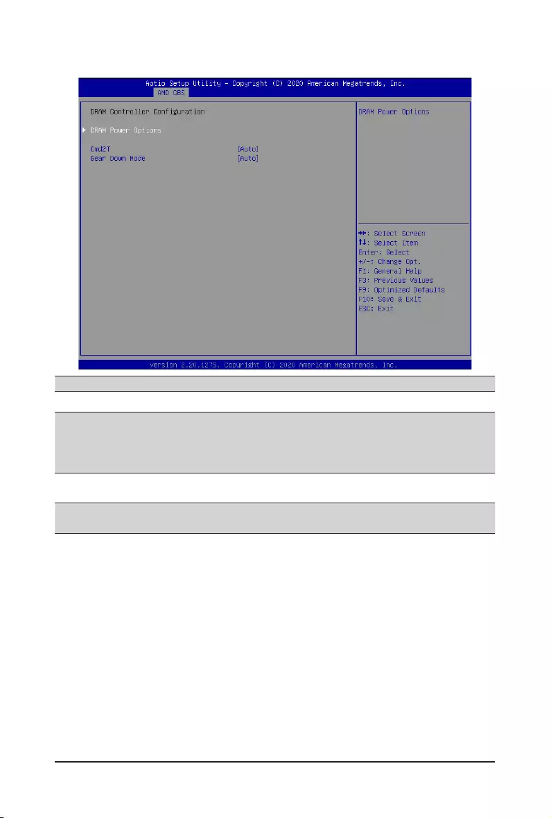
- 81 - BIOS Setup
2-3-3-1-1 DRAM Controller Conguration
Parameter Description
DRAMControllerConguration
DRAM Power Options
Press[Enter]tocongureDRAMPowerOptionsMa.
Power Down Enable
– Enable/Disable DDR power down mode.
– Options available: Auto, Enabled, Disabled. Default setting is Auto.
Cmd2T Selects the Cmd2T mode on ADDR/CMD.
Options available: Auto, 1T, 2T. Default setting is Auto.
Gear Down Mode Enable/Disable the Gear Down Mode function.
Options available: Auto, Enabled, Disabled. Default setting is Auto.
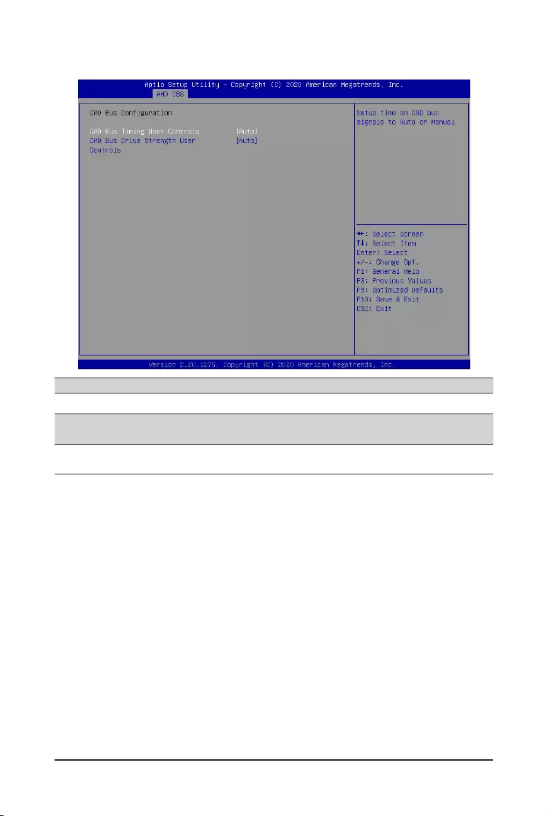
BIOS Setup - 82 -
2-3-3-1-2 CAD Bus Conguration
Parameter Description
CADBusConguration
CAD Bus Timing User Controls Setup time on CAD bus signals to Auto or Manual.
Options available: Auto, Manual. Default setting is Auto.
CAD Bus Drive Strength User
Controls
Drive Strength on CAD bus signals to Auto or Manual.
Options available: Auto, Manual. Default setting is Auto.
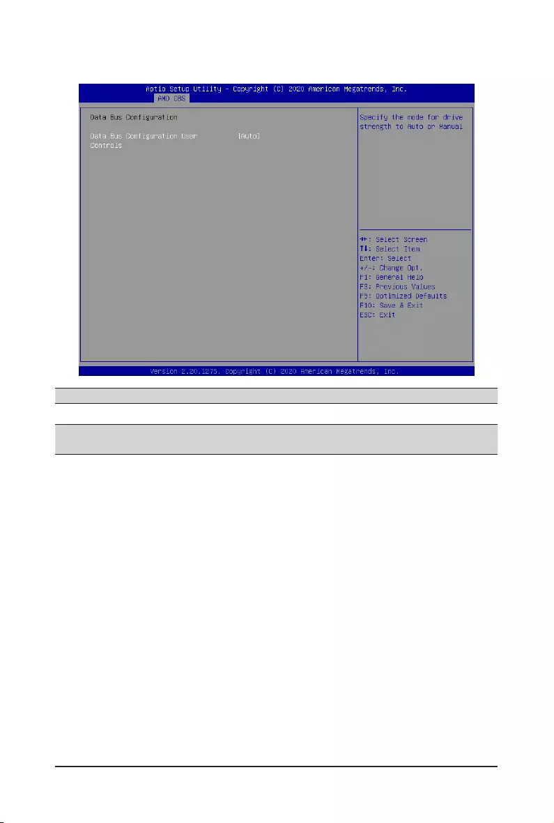
- 83 - BIOS Setup
2-3-3-1-3 Data Bus Conguration
Parameter Description
DataBusConguration
DataBusCongurationUser
Controls
SpeciesthemodefordrivestrengthtoAutoorManual.
Options available: Auto, Manual. Default setting is Auto.
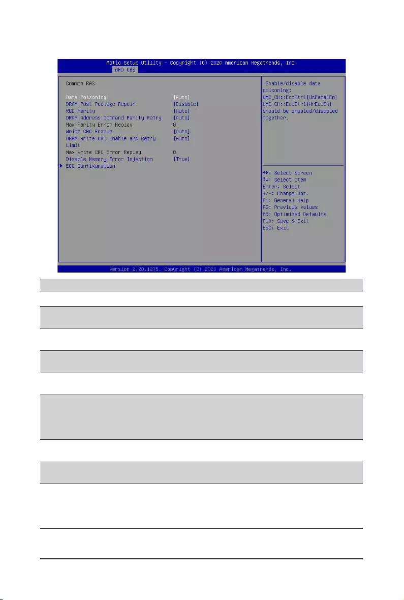
BIOS Setup - 84 -
2-3-3-1-4 Common RAS
Parameter Description
Common RAS
Data Poisoning Enable/Disable the Data Poisoning function.
Options available: Auto, Enabled, Disabled. Default setting is Auto.
DRAM Post Package Repair Enable/Disable the DRAM Post Package Repair function.
Options available: Enabled, Disabled. Default setting is Auto.
RCD Parity Enable/Disable the RCD Parity function.
Options available: Auto, Enabled, Disabled. Default setting is Auto.
DRAM Address Command Parity
Retry
Enable/Disable the DRAM Address Command Parity Retry function.
Options available: Auto, Enabled, Disabled. Default setting is Auto.
Max Parity Error Replay
CongurestheMaxParityErrorReplay.(0~0x3f)
Default setting is 8.
Please note that this item is congurable when DRAM Address
Command Parity Retry is set to Enabled.
Write CRC Enable Enable/Disable the Write CRC function.
Options available: Auto, Enabled, Disabled. Default setting is Auto.
DRAM Write CRC Enable and Retry
Limit
Enable/Disable DRAM Write CRC Enable and Retry Limit.
Options available: Auto, Enabled, Disabled. Default setting is Auto.
Max Write CRC Error Replay
CongurestheMaxWriteCRCErrorReplay.(0~0x3f)
Default setting is 8.
Please note that this item is congurable when DRAM Write CRC
Enable and Retry Limit is set to Enabled.

- 85 - BIOS Setup
Parameter Description
DisableMemoryErrorInjection Options available: False, True. Default setting is True.
ECCConguration
Press[Enter]tocongureadvanceditems.
DRAM ECC Symbol Size
– CongurestheDRAMECCSymbolSize.
– Options available: Auto, x4, x8, x16. Default setting is Auto.
DRAM ECC Enable
– Enable/Disable DRAM ECC. When set to Auto, it will set ECC
to enable.
– Options available: Auto, Enabled, Disabled. Default setting is
Auto.
DRAM UECC Retry
– Enable/Disable DRAM UECC Retry.
– Options available: Auto, Enabled, Disabled. Default setting is
Auto.
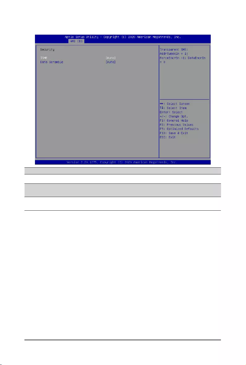
BIOS Setup - 86 -
2-3-3-1-5 Security
Parameter Description
Security
TSME Enable/Disable transparent secure memory encryption.
Options available: Auto, Enabled, Disabled. Default setting is Auto.
Data Scramble Enable/Disable Data Scrambling.
Options available: Auto, Enabled, Disabled. Default setting is Auto.
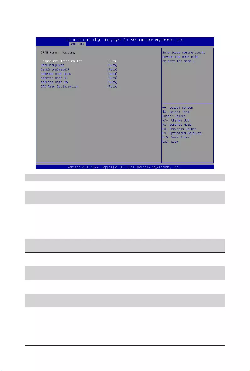
- 87 - BIOS Setup
2-3-3-2 DRAM Memory Mapping
Parameter Description
DRAM Memory Mapping
Chipselect Interleaving Interleave memory blocks across the DRAM chip selects for node 0.
Options available: Auto, Disabled. Default setting is Auto.
BankGroupSwap
CongurestheBankGroupSwap.BankGroupSwap(BGS)isanewmemory
mapping option in AGESA that alters how applications get assigned to
physical locations within the memory modules. When this option sets to
Auto, it is null: No help string.
Options available: Auto, Enabled, Disabled. Default setting is Auto.
BankGroupSwapAlt CongurestheBankGroupSwapAlt.
Options available: Auto, Enabled, Disabled. Default setting is Auto.
Address Hash Bank Enable/Disable bank address hashing.
Options available: Auto, Enabled, Disabled. Default setting is Auto.
Address Hash CS Enable/Disable CS address hashing.
Options available: Auto, Enabled, Disabled. Default setting is Auto
Address Hash Rm Enable/Disable RM address hashing.
Options available: Auto, Enabled, Disabled. Default setting is Auto
SPD Read Optimization Enable/Disable SPD Read Optimization.
Options available: Auto, Enabled, Disabled. Default setting is Auto
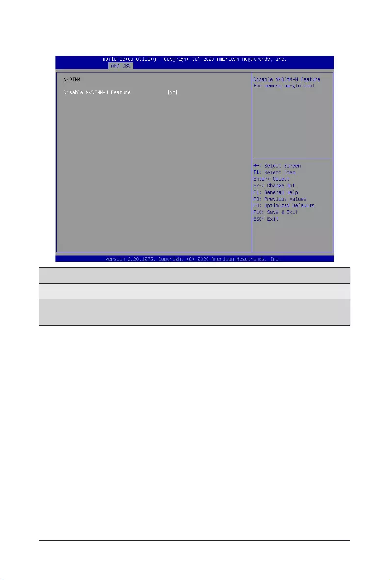
BIOS Setup - 88 -
2-3-3-3 NVDIMM
Parameter Description
NVDIMM Displays the information of the devices/controllers if installed
Disable NVDIMM-N
Feature
Enable/Disable NVDIMM-N feature for memory margin tool.
Options available: No, Yes. Default setting is NO.
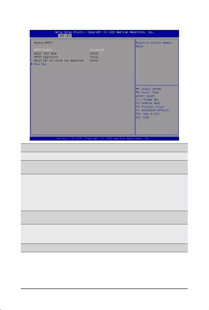
- 89 - BIOS Setup
2-3-3-4 Memory MBIST
Parameter Description
Memory MBIST
MBIST Enable Enable/Disable the Memory MBIST function.
Options available: Enabled, Disabled. Default setting is Disabled.
MBIST Test Mode(Note)
Selects MBIST Test Mode.
Interface Mode: Tests Single and Multiple CS transactions and Basic
Connectivity.
Data Eye Mode: Measures Voltage vs. Timing.
Options available: Auto, Both, Interface Mode, Data Eye Mode. Default
setting is Auto.
MBIST Aggressors(Note) Enable/Disable MBIST Aggressor test.
Options available: Auto, Enabled, Disabled. Default setting is Auto.
MBIST Per Bit Slave Die
Reporting(Note)
Enable/Disable to report 2D data eye results in ABL log for each DQ,
Chipselect, and Channel.
Options available: Auto, Enabled, Disabled. Default setting is Auto.
Data Eye Press[Enter]tocongureadvanceditems.
(Note) This item is available when MBIST Enable is set to Enabled.
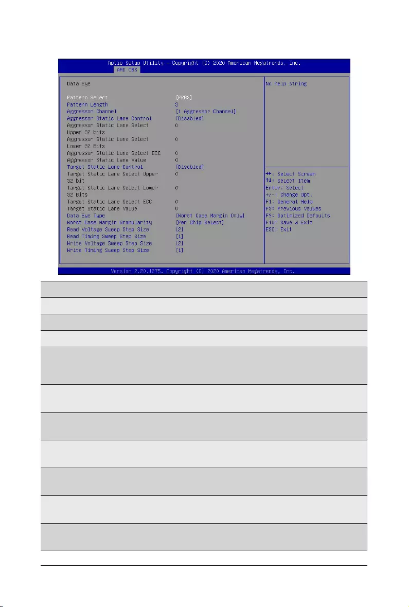
BIOS Setup - 90 -
2-3-3-4-1 Data Eye
Parameter Description
Data Eye
Pattern Select Options available: PRBS, SSO, Both. Default setting is PRBS.
Pattern Length Determines the pattern length. The possible options are N=3....12.
Aggressor Channel
This item helps read the aggressors channels.
Options available: Disabled, 1 Aggressor Channel, 3 Aggressor Channels,
7 Aggressor Channels. Default setting is 1 Aggressor Channel.
Aggressor Static Lane
Control
Enable/Disable the Aggressor Static Lane Control function.
Options available: Enabled, Disabled. Default setting is Disabled.
Aggressor Static Lane
Select Upper 32 bits
ThisitemiscongurablewhenAggressor Static Lane Control is set to
Enabled.
Aggressor Static Lane
Select Lower 32 bits
ThisitemiscongurablewhenAggressor Static Lane Control is set to
Enabled.
Aggressor Static Lane
Select ECC
ThisitemiscongurablewhenAggressor Static Lane Control is set to
Enabled.
Aggressor Static Lane
Value
ThisitemiscongurablewhenAggressor Static Lane Control is set to
Enabled.
Target Static Lane Control Enable/Disable the Target Static Lane Control function.
Options available: Enabled, Disabled. Default setting is Disabled.

- 91 - BIOS Setup
Parameter Description
Target Static Lane Select
Upper 32 bits
ThisitemiscongurablewhenTarget Static Lane Control is set to
Enabled.
Target Static Lane Select
Lower 32 bits
ThisitemiscongurablewhenTarget Static Lane Control is set to
Enabled.
Target Static Lane Select
ECC
ThisitemiscongurablewhenTarget Static Lane Control is set to
Enabled.
Target Static Lane Value ThisitemiscongurablewhenTarget Static Lane Control is set to
Enabled.
Data Eye Type
This item determines which results are expected to be captured for Data Eye.
Options available: 1D Voltage Sweep, 1D Timing Sweep, 2D Full Data Eye,
Worst Case Margin Only. Default setting is Worst Case Margin Only.
Worst Case Margin
Granularity
ConguresWorstCaseMarginGranularity.
Options available: Per Chip Select, Per Nibble.
Default setting is Worst Case Margin Only.
Read Voltage Sweep Step
Size
ConguresthestepsizeforreadDataEyevoltagesweep.
Options available: 1, 2, 4. Default setting is 2.
Read Timing Sweep Step
Size
ConguresthestepsizeforreadDataEyetimingsweep.
Options available: 1, 2, 4. Default setting is 1.
Write Voltage Sweep Step ConguresthestepsizeforwriteDataEyevoltagesweep.
Options available: 1, 2, 4. Default setting is 2.
Write Timing Sweep Step
Size
ConguresthestepsizeforwriteDataEyetimingsweep.
Options available: 1, 2, 4. Default setting is 1.
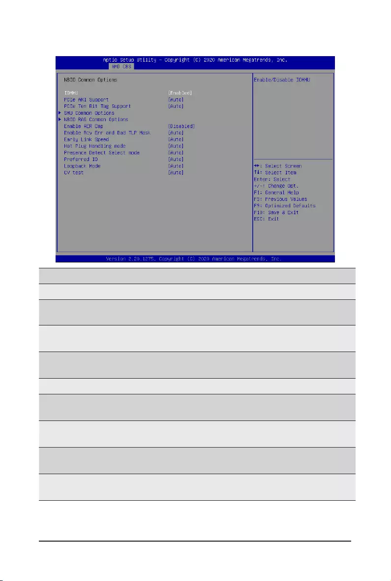
BIOS Setup - 92 -
2-3-4 NBIO Common Options
Parameter Description
NBIO Common Options
IOMMU Enable/Disable the IOMMU function.
Options available: Enabled, Disabled. Default setting is Disabled.
PCIe ARI Support Enable/Disable Alternative Routng-ID Interpretation.
Options available: Auto, Enabled, Disabled. Default setting is Auto.
PCIe Ten Bit Tag Support Enable/Disable PCIe ten bit tags for supported devices. (Auto=Disabled)
Options available: Auto, Enabled, Disabled. Default setting is Auto.
SMU Common Options Press[Enter]forcongurationofadvanceditems.
NBIO RAS Common
Options Press[Enter]forcongurationofadvanceditems.
Enable AER Cap Enable/Disable Advanced Error Reporting Capability.
Options available: Auto, Enabled, Disabled. Default setting is Auto.
Enable Rcv Err and Bad
TLP Mask
Enable/Disable Masking of Receiver Error and Bad TLP at Gen4 x2.
Options available: Auto, Enabled, Disabled. Default setting is Auto.
Early Link Speed ConguresEarlyLinkSpeed.
Options available: Auto, Gen1, Gen2. Default setting is Auto.

- 93 - BIOS Setup
Parameter Description
Hot Plug Handling mode
Controls the Hot Plug Handling mode.
Options available: Auto, A0 Mode, OS First (No Error Handling),
OS First (Error Handling-Not Implemented), Firmware First (Not Implemented).
Default setting is Auto.
Presence Detect Select
mode
Controls the Presence Detect Select mode.
Options available: Auto, OR, AND. Default setting is Auto.
Preferred IO
Preferred IO select type.
Manual: Bus Number manually.
Auto: Default.
Options available: Auto, Manual. Default setting is Auto.
Loopback Mode Enable/Disable the PCIe loopback mode.
Options available: Auto, Enabled, Disabled. Default setting is Auto.
CV test Enable/Disable the running PCIECV tool support.
Options available: Auto, Enabled, Disabled. Default setting is Auto.
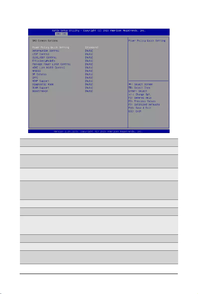
BIOS Setup - 94 -
2-3-4-1 SMU Common Options
Parameter Description
SMU Common Options
Power Policy Quick
Setting
Optionsavailable:Standard,BestPerformance,EnergyEfcient.
Default setting is Standard.
Determinism Control Selects use the fused Determinism or set customized Determinism.
Options available: Auto, Manual. Default setting is Auto.
cTDP Control
SelectsusethefusedTDPorsetcustomizedTDP.**TDPisusedtodenethe
RC thermal model only**
Options available: Auto, Manual. Default setting is Auto.
CLD0_VDDP Control Options available: Auto, Manual. Default setting is Auto.
EfciencyModeEn Options available: Auto, Enabled. Default setting is Auto.
Package Power Limit
Control
Selects use the fused PPT or set customized PPT. **PPT will be used as the
ASIC power limit**
Options available: Auto, Manual. Default setting is Auto.
xGMI Link Width Control Options available: Auto, Enabled. Default setting is Auto.
APBDIS Options available: Auto, 0, 1. Default setting is Auto.
DF Cstates Enable/Disable DF C-states.
Options available: Auto, Enabled, Disabled. Default setting is Auto.

- 95 - BIOS Setup
Parameter Description
CPPC Enable/Disable the CPPC feature.
Options available: Auto, Enabled, Disabled. Default setting is Auto.
HSMP Support Enable/Disable the HSMP support.
Options available: Auto, Enabled, Disabled. Default setting is Auto.
Diagnostic Mode Enable/Disable the Diagnostic Mode.
Options available: Auto, Enabled, Disabled. Default setting is Auto.
DLWM Support Enable/Disable the DLWM support.
Options available: Auto, Enabled, Disabled. Default setting is Auto.
BoostFmaxEn Options available: Auto, Enabled. Default setting is Auto.
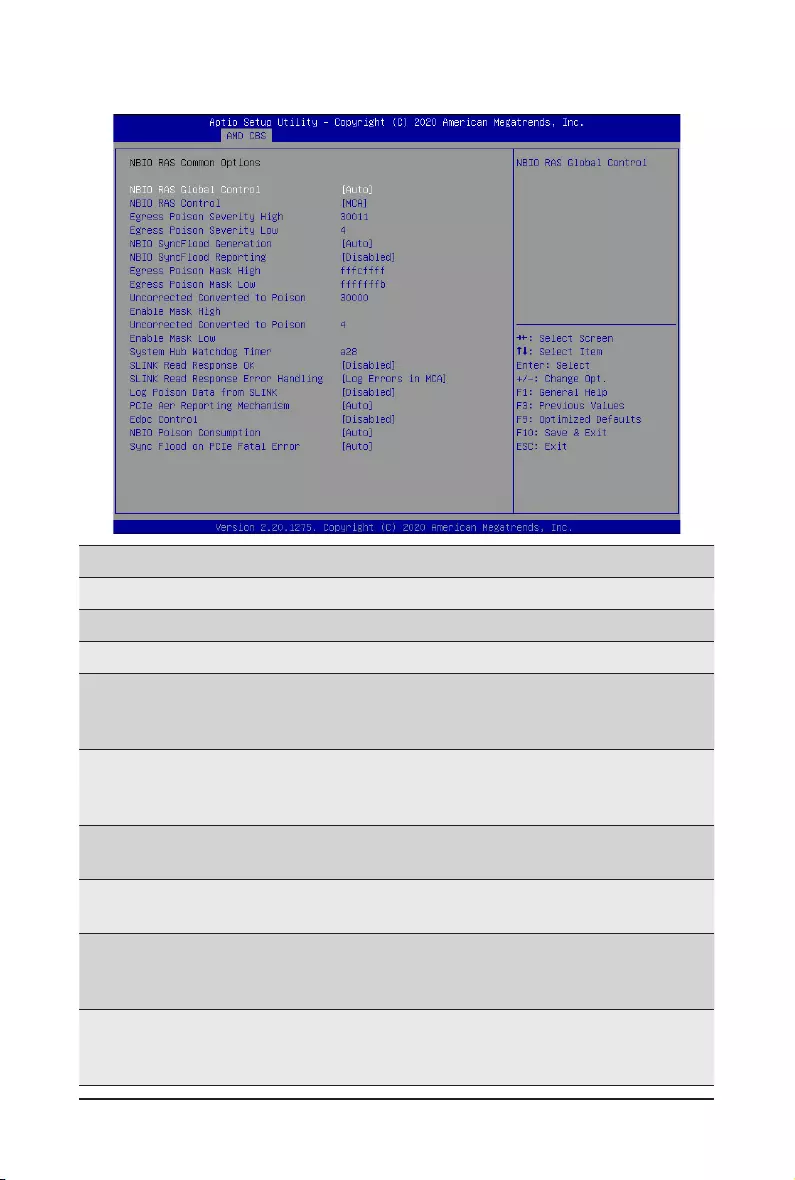
BIOS Setup - 96 -
2-3-4-2 NBIO RAS Common Options
Parameter Description
NBIO RAS Common Options
NBIO RAS Global Control Options available: Auto, Manual. Default setting is Auto.
NBIO RAS Control Options available: Disabled, MCA, Legacy. Default setting is MCA.
Egress Poison Serverity High
CongurestheEgressPoisonHighServerity.Eachbitsetto1enables
High serverity on the associated IOHC egress port. A bit of 0 indicates
LOW serverity.
Egress Poison Serverity Low
CongurestheEgressPoisonLowServerity.Eachbitsetto1enables
High serverity on the associated IOHC egress port. A bit of 0 indicates
LOW serverity.
NBIO SyncFlood Generation The value may be used to mask SyncFlood caused by NBIO RAS options.
Options available: Auto, Enabled, Disabled. Default setting is Auto.
NBIO SyncFlood Reporting The value may be used to enanle SyncFlood reporting to APML.
Options available: Enabled, Disabled. Default setting is Disabled.
Egress Poison Mask High
Enables mask for masking of errors logged in EGRESS_POISON_
STATUS. For each bit set to 1, errors are masked. For each bit set to 0,
errors trigger response actions.
Egress Poison Mask Low
Enables mask for masking of errors logged in EGRESS_POISON_
STATUS. For each bit set to 1, errors are masked. For each bit set to 0,
errors trigger response actions.

- 97 - BIOS Setup
Parameter Description
Uncorrected Converted to
Poison Enabke Mask High
Enables mask for masking of uncorrectable parity errors on internal
arrays.
Uncorrected Converted to
Poison Enabke Mask Low
Enables mask for masking of uncorrectable parity errors on internal
arrays.
System Hub Watchdog Timer SpeciesthetimerintervaloftheSYSHUBWatchdogtimerinmiliseconds.
SLINK Read Response OK
ThisitemspecieswhetherSLINKreadresponseerrorsareconvertedto
an Okay response.
Options available: Enabled, Disabled. Default setting is Disabled.
SLINK Read Response Error
Handling
Options available: Enabled, Trigger MCOMMIT Error, Log Errors in MCA.
Default setting is Log Errors in MCA.
Log Poison Data from SLINK Enable/Disable the Log Poison Data from SLINK feature.
Options available: Enabled, Disabled. Default setting is Disabled.
PCIe Aer Reporting
Mechanism
Selects the method of reporting AER errors from PCI Express.
Options available: Auto, Firmware First, OS First, MCA.
Default setting is Auto.
Edpc Control Options available: Auto, Enabled, Disabled. Default setting is Disabled.
NBIO Poison Consumption Options available: Auto, Enabled, Disabled. Default setting is Auto.
Sync Flood on PCIe Fatal
Error Options available: Auto, True, False. Default setting is Auto.
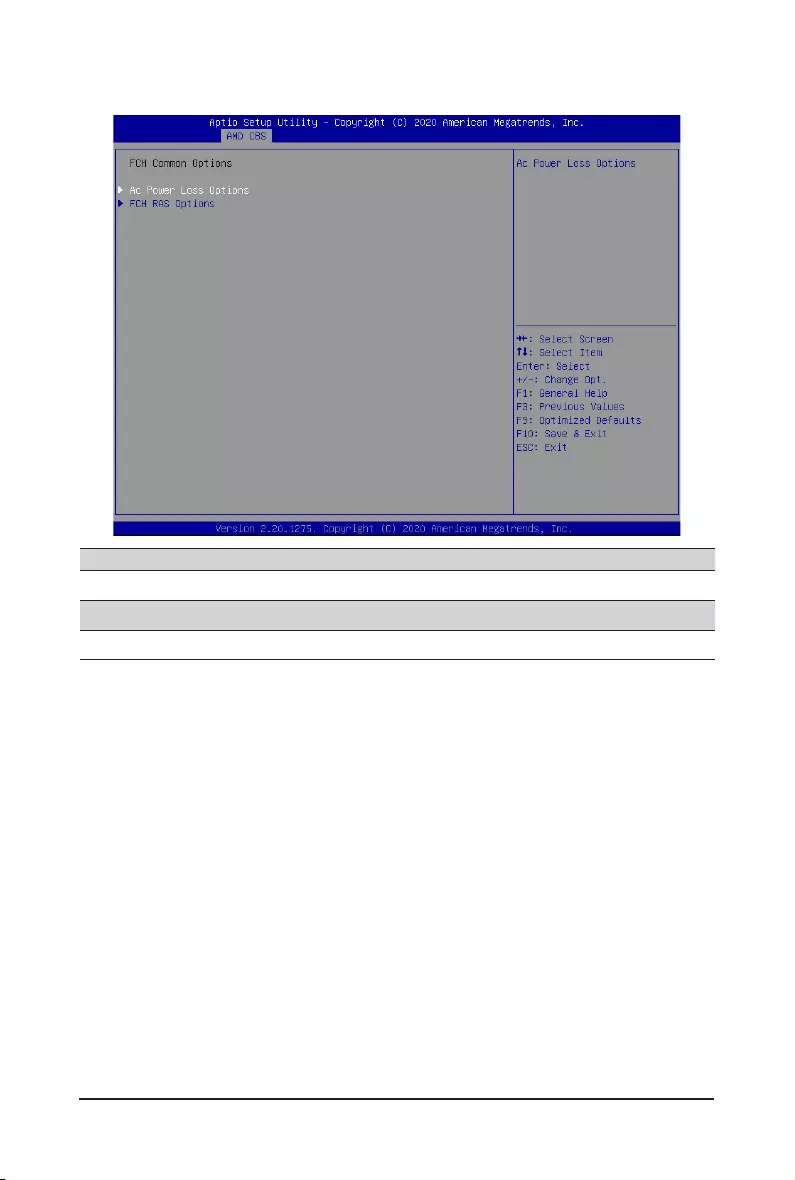
BIOS Setup - 98 -
2-3-5 FCH Common Options
Parameter Description
FCH Common Options
AC Power Loss Options Press[Enter]forcongurationofadvanceditems.
FCH RAS Options Press[Enter]forcongurationofadvanceditems.
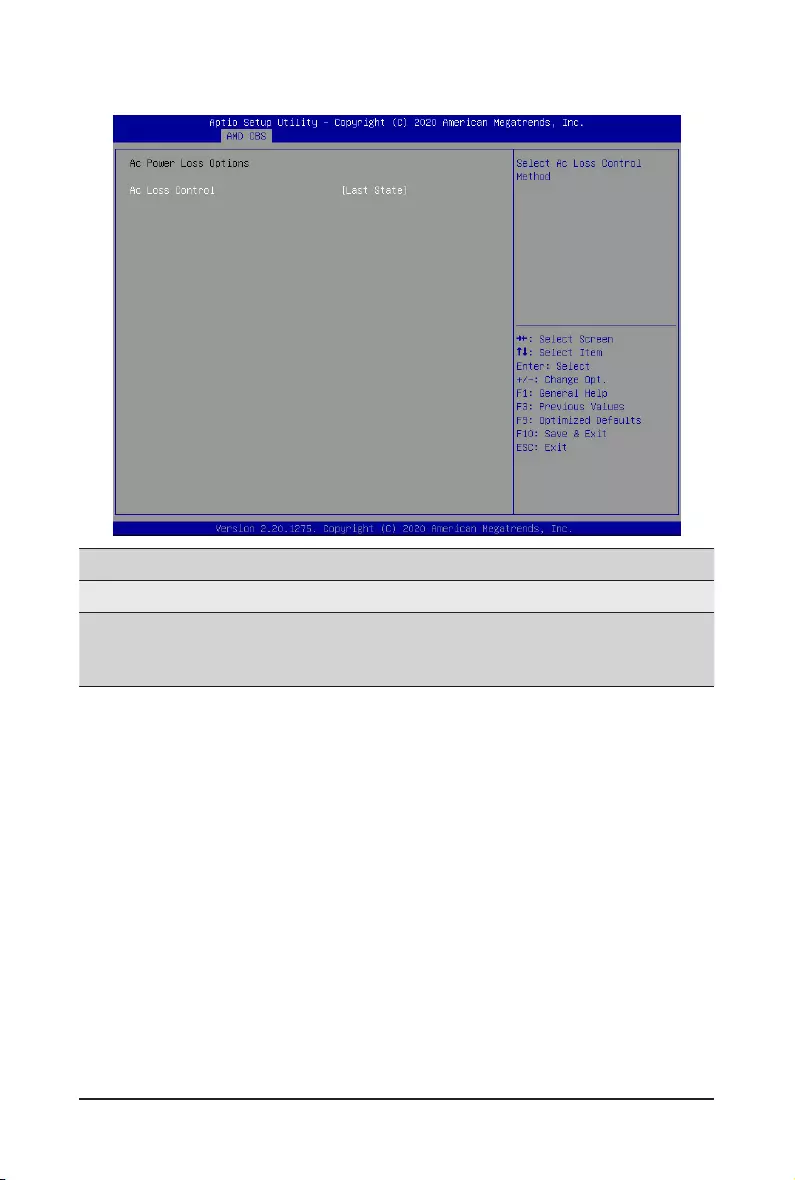
- 99 - BIOS Setup
2-3-5-1 AC Power Loss Options
Parameter Description
AC Power Loss Options
AC Loss Control
Selects the AC Loss Control Method.
Options available: Power Off, Power On, Last State.
Default setting is Last State.
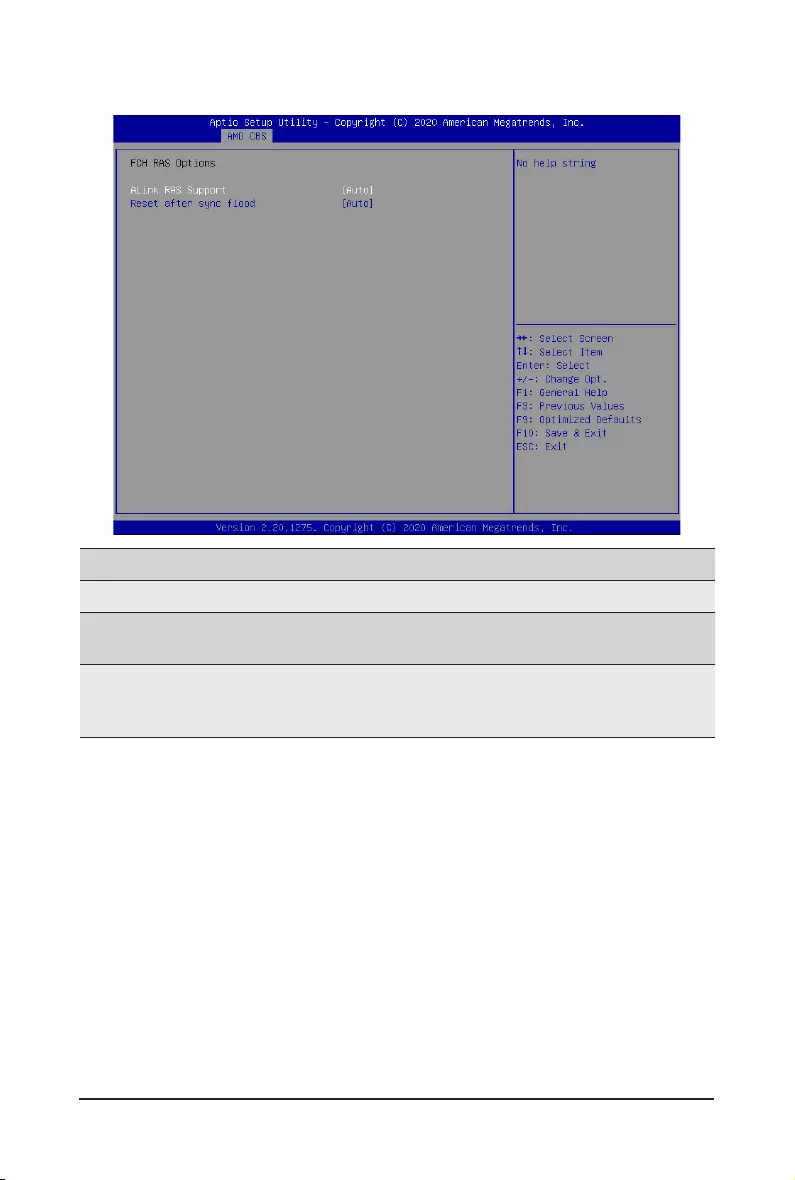
BIOS Setup - 100 -
2-3-5-2 FCH RAS Options
Parameter Description
FCH RAS Options
ALink RAS Support Enable/Disable the ALink RAS Support.
Options available: Auto, Enabled, Disabled. Default setting is Auto.
Resetaftersyncood
EnablesABtoforwarddownstreamsync-oodmessagetosystem
controller.
Options available: Auto, Enabled, Disabled. Default setting is Auto.
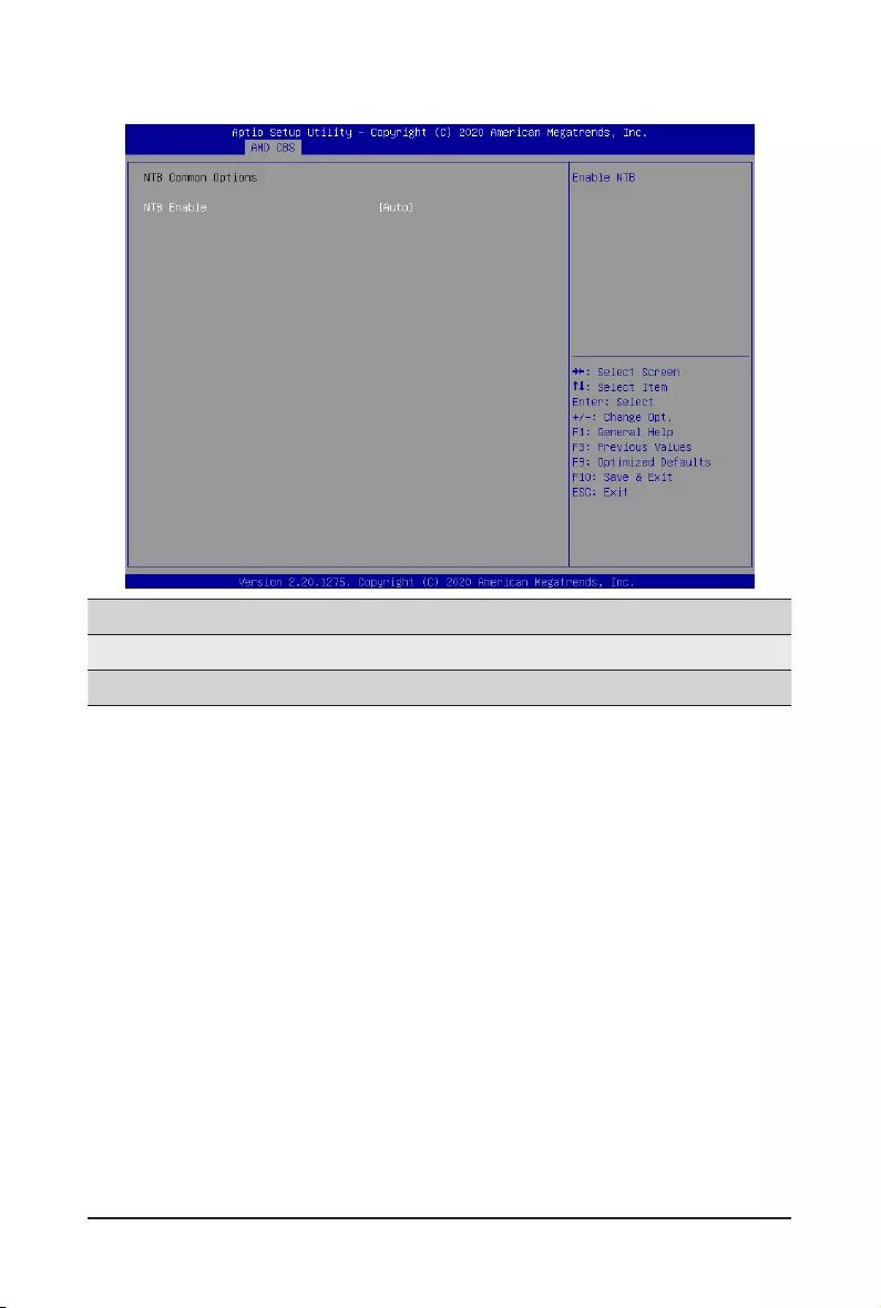
- 101 - BIOS Setup
2-3-6 NTB Common Options
Parameter Description
NTB Common Options
NTB Enable Options available: Auto, Enabled. Default setting is Auto.
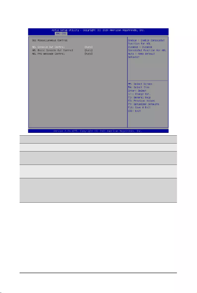
BIOS Setup - 102 -
2-3-7 SOC Miscellaneous Control
Parameter Description
SOC Miscellaneous Control
ABL Console Out Control Enable/Disable the ConsoleOut function for ABL.
Options available: Auto, Enabled, Disabled. Default setting is Auto.
ABL Basic Console Out
Control(Note)
Enable/Disable the Basic ConsoleOut function for ABL.
Options available: Auto, Enabled, Disabled. Default setting is Auto.
ABL PMU message
Control(Note)
To Control the total number of PMU debug messages.
Options available: Auto, Detailed debug message, Coarse debug
message, Stage completion, Firmware completion message only.
Default setting is Auto.
(Note) ThisitemiscongurablewhenABL Console Out Control is set to Enabled.
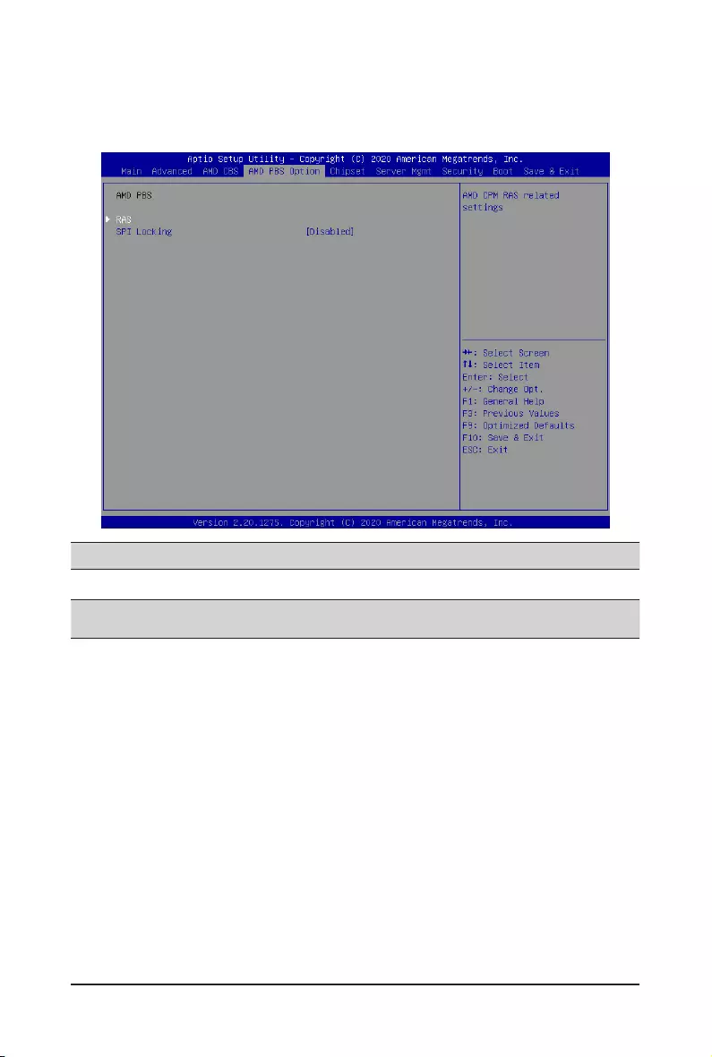
- 103 - BIOS Setup
2-4 AMD PBS Menu
AMD PBS Option menu displays submenu options for configuring the function of AMD PBS. Select a
submenu item, then press [Enter] to access the related submenu screen.
Parameter Description
RAS Press[Enter]forcongurationofadvanceditems.
SPI Locking Enable/Disable SPI Locking for protect ROM part.
Options available: Enabled, Disabled. Default setting is Disabled.
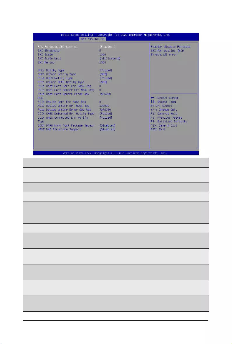
BIOS Setup - 104 -
2-4-1 RAS
Parameter Description
RAS Periodic SMI Control Enable/Disable the Periodic SMI for polling [MCA Threshold] error.
Options available: Enabled, Disabled. Default setting is Enabled.
SMI Threshold CongurestheSMIThresholdvalue.
SMI Scale CongurestheSMIScalevalue.
SMI Scale Unit
Denestheunitoftimescale.
Options available: millisecond, second, minute. Default setting is
millsecond.
SMI Period CongurestheSMIPeriod.
GHES Notify Type SelectstheNoticationtypefordeferred/correctederrors.
Options available: Polled, SCI. Default setting is Polled.
GHES UnCorr Notify Type SelectstheNoticationtypeforuncorrectederrors.
Options available: Polled, NMI. Default setting is NMI.
PCIe GHES Notify Type SelectstheNoticationtypeforPCIecorrectederrors.
Options available: Polled, SCI. Default setting is Polled.
PCIe UnCorr GHES Notify
Type
SelectstheNoticationtypeforPCIeuncorrectederrors.
Options available: Polled, NMI. Default setting is NMI.
PCIe Root Port Corr Err
Mask Reg Initialize the PCIe AER Corrected Error Mask register of Root Port.

- 105 - BIOS Setup
Parameter Description
PCIe Root Port UnCorr Err
Mask Reg Initialize the PCIe AER Uncorrected Error Mask register of Root Port.
PCIe Root Port UnCorr Err
Sev Reg Initialize the PCIe AER Uncorrected Error Serverity register of Root Port.
PCIe Device Corr Err Mask
Reg Initialize the PCIe AER Corrected Error Mask register of PCIe device.
PCIe Device UnCorr Err
Mask Reg Initialize the PCIe AER Uncorrected Error Mask register of PCIe device.
PCIe Device UnCorr Err Sev
Reg
Initialize the PCIe AER Uncorrected Error Serverity register of PCIe
device.
CCIX GHES Deferred ERR
Notify Type
SelectstheNoticationtypeforCCIXdefferederror.
Options available: Polled, SCI. Default setting is Polled.
CCIX GHES Corrected Err
Notify Type
SelectstheNoticationtypeforCCIXcorrectederror.
Options available: Polled, SCI. Default setting is Polled.
DDR4 DRAM Hard Post
Package Repair
This feature allows spare DRAM rows to replace malfunctioning rows via
anin-eldrepairmechanism.
Options available: Enabled, Disabled. Default setting is Disabled.
HEST DMC Structure
Support
HEST DMC (Deferred Machine Check) Structure Support.
Options available: Enabled, Disabled. Default setting is Disabled.
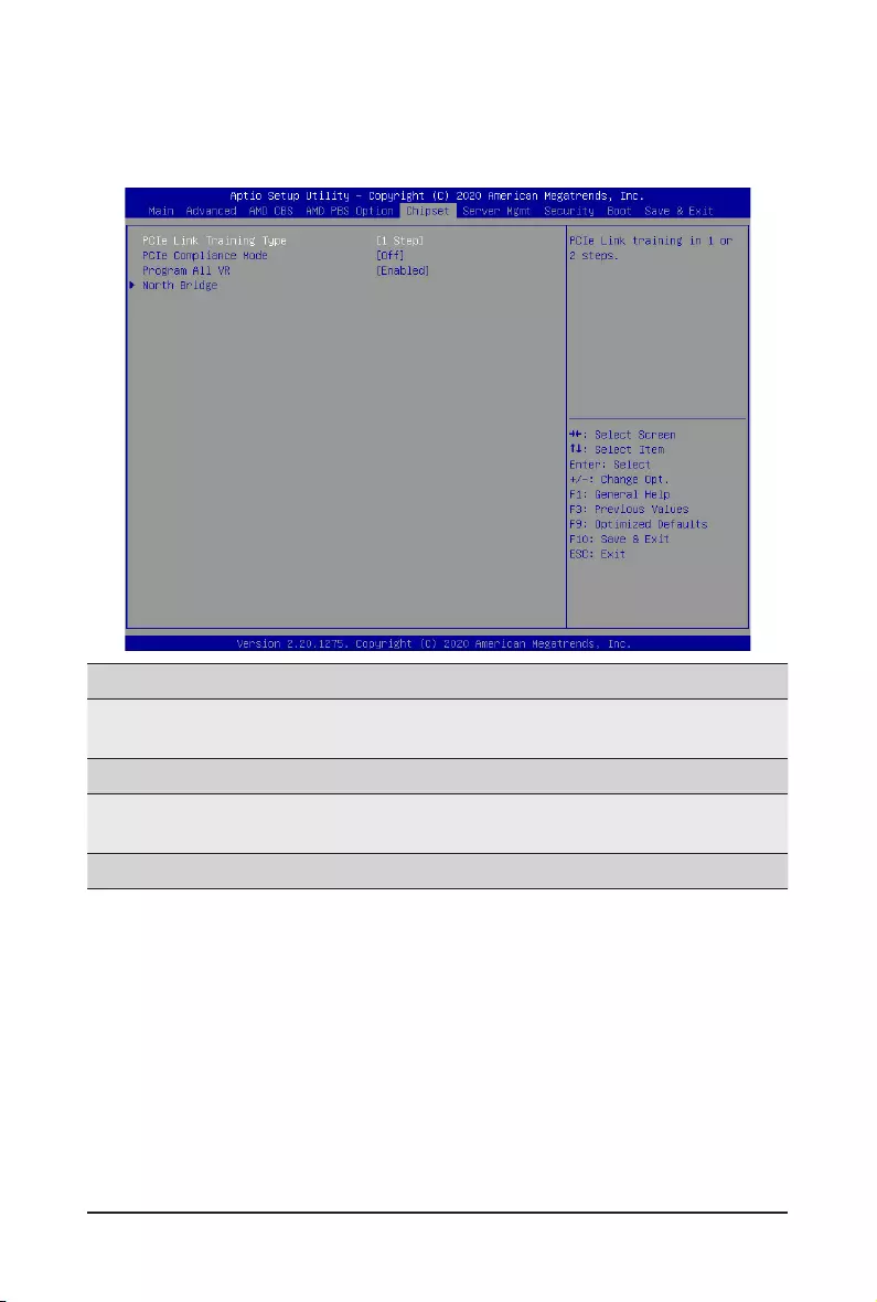
BIOS Setup - 106 -
2-5 Chipset Setup Menu
ChipsetSetupmenudisplayssubmenuoptionsforconguringthefunctionoftheNorthBridge.
Select a submenu item, then press <Enter> to access the related submenu screen.
Parameter Description
PCIe Link Training Type ConguresthePCIeLinktrainingin1or2steps.
Options available: 1 Step, 2Step. Default setting is 1 Step.
PCIe Compliance Mode Options available: On, Off. Default setting is Off.
Program All VR Enable/Disable program all VR on MB.
Options available: Enabled, Disabled. Default setting is Enabled.
North Bridge Press[Enter]forcongurationofadvanceditems.
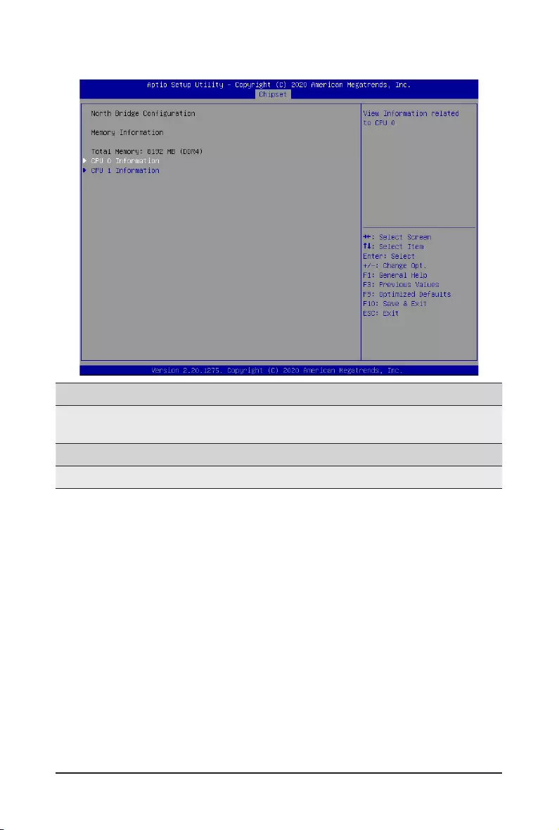
- 107 - BIOS Setup
2-5-1 North Bridge
Parameter Description
NorthBridgeConguration
Memory Information
Total Memory Displays the total memory information.
CPU0/1 Information Press [Enter] to view information related to CPU 0/1.
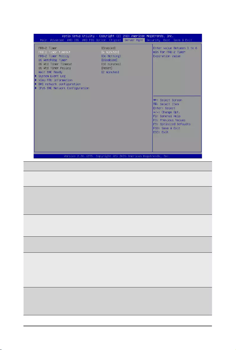
BIOS Setup - 108 -
2-6 Server Management Menu
Parameter Description
FRB-2 Timer Enable/Disable FRB-2 timer (POST timer).
Options available: Enabled, Disabled. Default setting is Enabled.
FRB-2 Timer
timeout
CongurestheFRB2Timertimeout.
Options available: 3 minutes, 4 minutes, 5 minutes, 6 minutes. Default setting is 6
minutes.
Please note that this item is congurable when FRB-2 Timer is set to Enabled.
FRB-2 Timer Policy
CongurestheFRB2Timerpolicy.
Options available: Do Nothing, Reset, Power Down. Default setting is Do Nothing.
Please note that this item is congurable when FRB-2 Timer is set to Enabled.
OS Watchdog
Timer
Enable/Disable OS Watchdog Timer function.
Options available: Enabled, Disabled. Default setting is Disabled.
OS Wtd Timer
Timeout
ConguresOSWatchdogTimer.
Options available: 5 minutes, 10 minutes, 15 minutes, 20 minutes. Default setting is
10 minutes.
Please note that this item is congurable when OS Watchdog Timer is set to
Enabled.
OS Wtd Timer
Policy
CongureOSWatchdogTimerPolicy.
Options available: Reset, Do Nothing, Power Down. Default setting is Reset.
Please note that this item is congurable when OS Watchdog Timer is set to
Enabled.

- 109 - BIOS Setup
Parameter Description
System Event Log Press[Enter]tocongureadvanceditems.
View FRU
Information Press [Enter] to view the FRU information.
BMC network
conguration Press[Enter]tocongureadvanceditems.
IPv6 BMC Network
Conguration Press[Enter]tocongureadvanceditems.
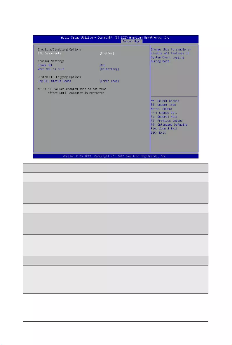
BIOS Setup - 110 -
2-6-1 System Event Log
Parameter Description
Enabling / Disabling Options
SEL Components
Change this item to enable or disable all features of System Event
Logging during boot.
Options available: Enabled, Disabled. Default setting is Enabled.
Erasing Settings
Erase SEL
Choose options for erasing SEL.
Options available: No/Yes, On next reset/Yes, On every reset. Default
setting is No.
When SEL is Full
Choose options for reactions to a full SEL.
Options available: Do Nothing, Erase Immediately. Default setting is Do
Nothing.
Custom EFI Logging Options
Log EFI Status Codes
Enable/Disable the logging of EFI Status Codes (if not already converted
to legacy).
Options available: Disabled, Both, Error code, Progress code. Default
setting is Error code.
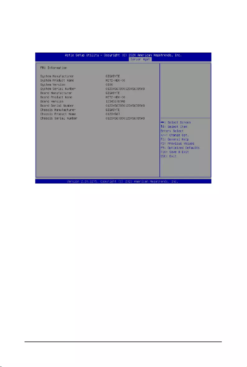
- 111 - BIOS Setup
2-6-2 View FRU Information
The FRU page is a simple display page for basic system ID information, as well as System product
information.Itemsonthiswindowarenon-congurable.
(Note) The model name will vary depends on the product you purchased
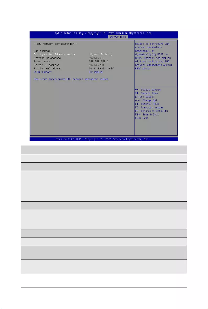
BIOS Setup - 112 -
2-6-3 BMC Network Conguration
Parameter Description
BMCnetworkconguration
Lan Channel 1
CongurationAddresssource
SelectstocongureLANchannelparametersstaticallyordynamically
(DHCP). Do nothing option will not modify any BMC network parameters
during BIOS phase.
Optionsavailable:Unspecied,Static,DynamicBmcDhcp.Defaultsetting
is DynamicBmcDhcp.
Station IP address Displays IP Address information.
Subnet mask
Displays Subnet Mask information.
Please note that the IP address must be in three digitals, for example,
192.168.000.001.
Router IP address Displays the Router IP Address information.
Station MAC address Displays the MAC Address information.
VLAN Support Set BMC to enable/disable VLAN support.
Options available: Enabled, Disabled. Default setting is Enabled.
Real-time get BMC network
address
Press [Enter] will set LAN mode and Address source and then get IP,
Subnet, Gateway and MAC address.
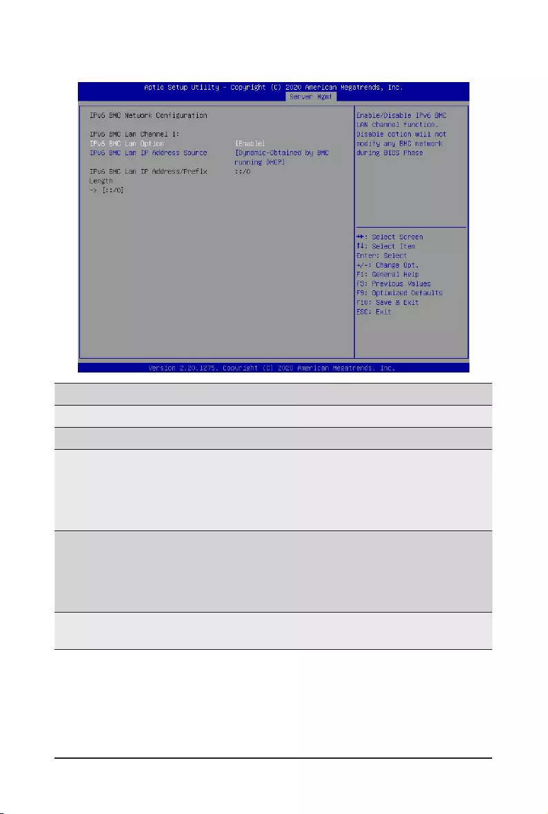
- 113 - BIOS Setup
2-6-4 IPv6 BMC Network Conguration
Parameter Description
IPv6BMCnetworkconguration
IPv6 BMC Lan Channel 1
IPv6 BMC Lan Option
Enable/Disable IPv6 BMC LAN channel function. When this item is
disabled, the system will not modify any BMC network during BIOS
phase.
Optionsavailable:Unspecied,Disable,Enable.Defaultsettingis
Enable.
IPv6 BMC Lan IP Address
Source
SelectstocongureLANchannelparametersstaticallyordynamically(by
BIOS or BMC).
Optionsavailable:Unspecied,Static,Dynamic-ObtainedbyBMC
running DHCP. Default setting is Enable Dynamic-Obtained by BMC
running DHCP.
IPv6 BMC Lan IP Address/
PrexLength
Check if the IPv6 BMC LAN IP address matches those displayed on the
screen.
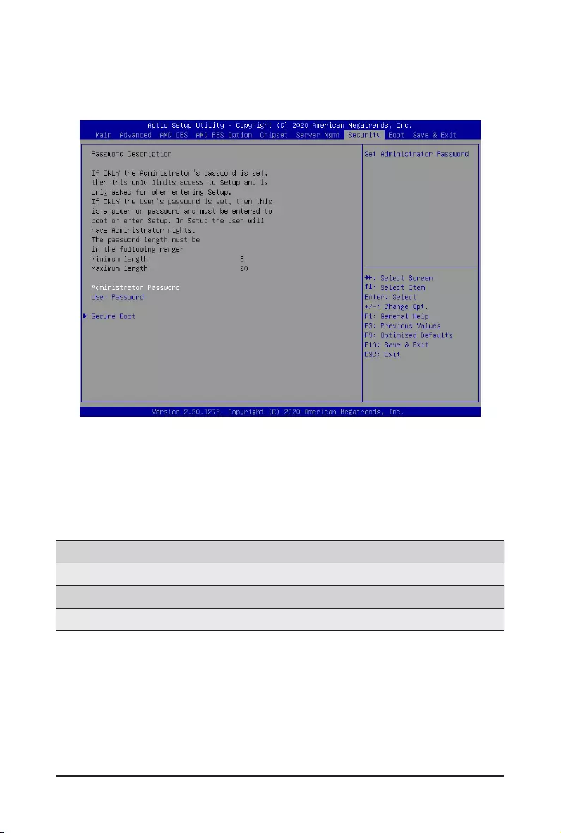
BIOS Setup - 114 -
2-7 Security Menu
The Security menu allows you to safeguard and protect the system from unauthorized use by setting up
access passwords.
There are two types of passwords that you can set:
• Administrator Password
Entering this password will allow the user to access and change all settings in the Setup Utility.
• User Password
Entering this password will restrict a user’s access to the Setup menus. To enable or disable
thiseld,aAdministratorPasswordmustrstbeset.Ausercanonlyaccessandmodifythe
SystemTime,SystemDate,andSetUserPasswordelds.
Parameter Description
Administrator Password Press[Enter]toconguretheadministratorpassword.
User Password Press[Enter]toconguretheuserpassword.
Secure Boot Press[Enter]tocongureadvanceditems.
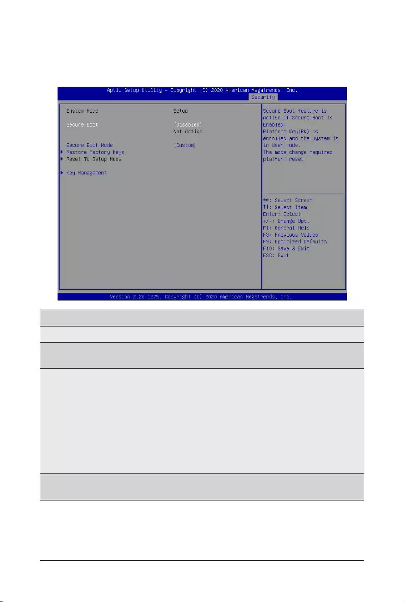
- 115 - BIOS Setup
2-7-1 Secure Boot
The Secure Boot submenu is applicable when your device is installed the Windows® 8 (or above) operating
system.
(Note) Advanced items prompt when this item is set to Custom.
Parameter Description
System Mode Displays if the system is in User mode or Setup mode.
Secure Boot Enable/ Disable the Secure Boot function.
Options avaiable:Enabled, Disabled. Default setting is Disabled.
Secure Boot Mode(Note)
Secure Boot requires all the applications that are running during the
bootingprocesstobepre-signedwithvaliddigitalcerticates.Thisway,
thesystemknowsalllesbeingloadedbeforeWindowsloadstothelogin
screen have not been tampered with.
When set to Standard, it will automatically load the Secure Boot keys
form the BIOS databases.
When set to Custom, you can customize the Secure Boot settings and
manually load its keys from the BIOS database.
Options available: Standard, Custom. Default setting is Standard.
Restore Factory Keys Forces the system to user mode and installs factury default Secure Boot
key database.

BIOS Setup - 116 -
Parameter Description
Key Management
Press[Enter]tocongureadvanceditems.
Please note that this item is congurable when Secure Boot Mode is set
to Custom.
Factory Key Provision
– Allows to provision factory default Secure Boot keys when system is in
Setup Mode.
– Options available: Enabled, Disabled. Default setting is Disabled.
Restore Factory Keys
– Installs all factory default keys. It will force the system in User Mode.
– Options available: Yes, No.
EnrollEImage
– Press [Enter] to enroll SHA256 hash of the binary into Authorized
Signature Database (db).
Restore DB defaults
– Restore DB variable to factory defaults.
Secure Boot variable
– Displays the current status of the variables used for secure boot.
Platform Key (PK)
– Displays the current status of the Platform Key (PK).
– Press[Enter]tocongureanewPK.
– Options available: Update.
Key Exchange Keys (KEK)
– Displays the current status of the Key Exchange Key Database (KEK).
– Press[Enter]tocongureanewKEKorloadadditionalKEKfrom
storage devices.
– Options available: Update, Append.
Authorized Signatures (DB)
– Displays the current status of the Authorized Signature Database.
– Press[Enter]tocongureanewDBorloadadditionalDBfromstorage
devices.
– Options available: Update, Append.
Forbidden Signatures (DBX)
– Displays the current status of the Forbidden Signature Database.
– Press[Enter]tocongureanewdbxorloadadditionaldbxfrom
storage devices.
– Options available: Update, Append.
Authorized TimeStamps (DBT)
– Displays the current status of the Authorized TimeStamps Database.
– Press[Enter]tocongureanewDBTorloadadditionalDBTfrom
storage devices.
– Options available: Update, Append.
OsRecovery Signatures
– Displays the current status of the OsRecovery Signature Database.
– Press[Enter]tocongureanewOsRecoverySignatureorload
additional OsRecovery Signature from storage devices.
– Options available: Update, Append.
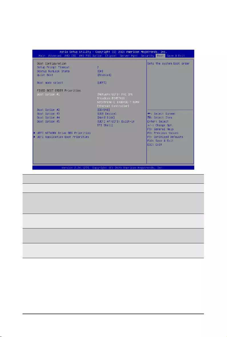
- 117 - BIOS Setup
2-8 Boot Menu
The Boot menu allows you to set the drive priority during system boot-up. BIOS setup will display an error
messageifthelegacydrive(s)speciedisnotbootable.
Parameter Description
BootConguration
Setup Prompt Timeout
Number of seconds to wait for setup activation key. 65535 (0xFFFF)
meansindenitewaiting.
Press the numeric keys to input the desired values.
Bootup NumLock State Enable/Disable the Bootup NumLock function.
Options available: On, Off. Default setting is Off.
Quiet Boot Enable/Disable showing the logo during POST.
Options available: Enabled, Disabled. Default setting is Enabled.
Boot mode select Selects the boot mode.
Options available: LEGACY, UEFI. Default setting is UEFI.

BIOS Setup - 118 -
Parameter Description
FIXED BOOT ORDER Priorities
Boot Option #1 / #2 / #3 / #4 / #5
Press[Enter]tocongurethebootpriority.
By default, the server searches for boot devices in the following
sequence:
1. Hard drive.
2. CD-COM/DVD drive.
3. USB device.
4. Network.
5. UEFI.
UEFI Network Drive BBS
Priorities Press[Enter]tocongurethebootpriority.
UEFI Application Boot Priorities Press[Enter]tocongurethebootpriority.
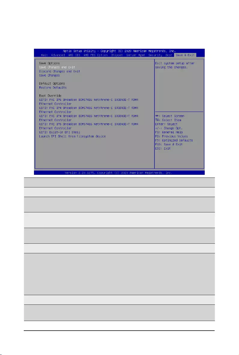
- 119 - BIOS Setup
2-9 Save & Exit Menu
The Save & Exit menu displays the various options to quit from the BIOS setup. Highlight any of the exit
options then press <Enter>.
Parameter Description
Save Options
Save Changes and Exit Saves changes made and closes the BIOS setup.
Options available: Yes, No.
Discard Changes and Exit Discards changes made and exits the BIOS setup.
Options available: Yes, No.
Save Changes Saves changes done so far to any of the setup options.
Options available: Yes, No.
Default Options
Restore Defaults
Loads the default settings for all BIOS setup parameters. Setup Defaults
are quite demanding in terms of resources consumption. If you are using
low-speed memory chips or other kinds of low-performance components
and you choose to load these settings, the system might not function
properly.
Options available: Yes, No.
Boot Override Press[Enter]tocongurethedeviceastheboot-updrive.
Launch EFI Shell from
lesystemdevice
AttemptstoLaunchEFIShellapplication(Shell.e)fromoneofthe
availablelesystemdevices.

BIOS Setup - 120 -
2-10 ABL POST Codes
2-10-1 StartProcessorTestPoints
Entry used for range testing for @b Processor related TPs 0xE000
2-10-2 Memory test points
Memory structure initialization (Public interface) 0xE001
SPD Data processing (Public interface) 0xE002
Memoryconguration(Publicinterface)Phase1 0xE003
DRAM initialization 0xE004
ProcMemSPDChecking 0xE005
ProcMemModeChecking 0xE006
SpeedandTCLconguration 0xE007
ProcMemSpdTiming 0xE008
ProcMemDramMapping 0xE009
ProcMemPlatformSpecicCong 0xE00A
ProcMemPhyCompensation 0xE00B
ProcMemStartDcts 0xE00C
ProcMemBeforeDramInit (Public interface) 0xE00D
ProcMemPhyFenceTraining 0xE00E
ProcMemSynchronizeDcts 0xE00F
ProcMemSystemMemoryMapping 0xE010
ProcMemMtrrConguration 0xE011
ProcMemDramTraining 0xE012
ProcMemBeforeAnyTraining(Public interface) 0xE013
2-10-3 PMU Test Points
ABL Mem - PMU - Before PMU Firmware load 0xE014
ABL Mem - PMU - After PMU Firmware load 0xE015
ABL Mem - PMU Populate SRAM Timing 0xE016
ABLMem-PMUPopulateSRAMCong 0xE017
ABL Mem - PMU Write SRAM Msg Block 0xE018
ABL Mem - Wait for Phy Cal Complete 0xE019
ABL Mem - Phy Cal Complete 0xE01A
ABL Mem - PMU Start 0xE01B
ABL Mem - PMU Started 0xE01C
ABL Mem - PMU Waiting for Complete 0xE01D
ABL Mem - PMU Stage Dec Init 0xE01E
ABL Mem - PMU Stage Training Wr Lvl 0xE01F
ABL Mem - PMU Stage Training Rx En 0xE020
ABL Mem - PMU Stage Training Rd Dqs 0xE021
ABL Mem - PMU Stage Traning Rd 2D 0xE022

- 121 - BIOS Setup
ABL Mem - PMU Stage Training Wr 2D 0xE023
ABL Mem - PMU Queue Empty 0xE024
ABL Mem - PMU US message Start 0xE025
ABL Mem - PMU US message End 0xE026
ABL Mem - PMU Complete 0xE027
ABL Mem - PMU - After PMU Training 0xE028
ABL Mem - PMU - Before Disable PMU 0xE029
2-10-4 Original Post Code
ProcMemTransmitDqsTraining 0xE02A
ABL Mem - Start write sweep 0xE02B
ABL Mem - Set Transmit DQ delay 0xE02C
ABL Mem - Write test pattern 0xE02D
ABL Mem - Read Test pattern 0xE02E
ABL Mem - Compare Test pattern 0xE02F
ABL Mem - Update results 0xE030
ABL Mem - Start Find passing window 0xE031
ABL Mem - ProcMemMaxRdLatencyTraining 0xE032
ABL Mem - Start sweep 0xE033
ABL Mem - Set delay 0xE034
ABL Mem - Write test pattern 0xE035
ABL Mem - Read Test pattern 0xE036
ABL Mem - Compare Test pattern 0xE037
ABL Mem - Online Spare init 0xE038
ABL Mem - Chip select Interleave Init 0xE039
ABL Mem - Node Interleave Init 0xE03A
ABL Mem - Channel Interleave Init 0xE03B
ABL Mem - ECC initialization 0xE03C
ABLMem-PlatformSpecicInit 0xE03D
ABL Mem - Before callout for "AgesaReadSpd" 0xE03E
ABL Mem - After callout for "AgesaReadSpd" 0xE03F
ABL Mem - Before optional callout "AgesaHookBeforeDramInit" 0xE040
ABL Mem - After optional callout "AgesaHookBeforeDramInit" 0xE041
ABL Mem - Before optional callout "AgesaHookBeforeDQSTraining" 0xE042
ABL Mem - After optional callout "AgesaHookBeforeDQSTraining" 0xE043
ABL Mem - Before optional callout "AgesaHookBeforeDramInit" 0xE044
ABL Mem - After optional callout "AgesaHookBeforeDramInit" 0xE045
ABL Mem - After MemDataInit 0xE046
ABL Mem - Before InitializeMCT 0xE047
ABL Mem - Before LV DDR3 0xE048
ABL Mem - Before InitMCT 0xE049

BIOS Setup - 122 -
ABL Mem - Before OtherTiming 0xE04A
ABL Mem - Before UMAMemTyping 0xE04B
ABL Mem - Before SetDqsEccTmgs 0xE04C
ABL Mem - Before MemClr 0xE04D
ABL Mem - Before On DIMM Thermal 0xE04E
ABL Mem - Before DMI 0xE04F
ABL MEM - End of phase 3 memory code 0xE050
2-10-5 CPU test points
Entry point CPU init after training 0xE051
Exit point CPU init after training 0xE052
Entry point CPU APOB CCX map init 0xE053
Exit point CPU APOB CCX map init 0xE054
Entry point CPU Optimized boot init 0xE055
Exit point CPU Optimized boot init 0xE056
Entry point CPU APOB EDC info init 0xE057
Exit point CPU APOB EDC info init 0xE058
2-10-6 Topology test points
ProcTopologyEntry 0xE071
ProcTopologyDone 0xE07C
2-10-7 Extended memory test point
ProcMemSendMRS2 0xE080
Sedding MRS3 0xE081
Sending MRS1 0xE082
Sending MRS0 0xE083
Continuous Pattern Read 0xE084
Continuous Pattern Write 0xE085
Mem: 2d RdDqs Training begin 0xE086
Mem: Before optional callout to platform BIOS to change External Vref
during 2d Training
0xE087
Mem: After optional callout to platform BIOS to change External Vref during
2d Training
0xE088
CongureDCTForGeneralusebegin 0xE089
CongureDCTFortrainingbegin 0xE08A
CongureDCTForNon-Explicit 0xE08B
ConguretoSyncchannels 0xE08C
Allocate C6 Storage 0xE08D
Before LV DDR4 0xE08E
Before LV DDR3 0xE08F

- 123 - BIOS Setup
2-10-8 Gnb Earlier init
TP0x90 0xE090
GNB earlier interface 0xE091
GNB internal debug code 0xE092
GNB internal debug code 0xE093
GNB internal debug code 0xE094
GNB internal debug code 0xE095
GNB internal debug code 0xE096
GNB internal debug code 0xE097
GNB internal debug code 0xE098
GNB internal debug code 0xE099
GNB internal debug code 0xE09A
GNB internal debug code 0xE09B
GNB internal debug code 0xE09C
GNB internal debug code 0xE09D
GNB internal debug code 0xE09E
GNB internal debug code 0xE09F
TP0xA0 0xE0A0
GNB internal debug code 0xE0A1
GNB internal debug code 0xE0A2
GNB internal debug code 0xE0A3
GNB internal debug code 0xE0A4
GNB internal debug code 0xE0A5
GNB internal debug code 0xE0A6
GNB internal debug code 0xE0A7
GNB internal debug code 0xE0A8
GNB internal debug code 0xE0A9
GNB internal debug code 0xE0AA
GNB internal debug code 0xE0AB
GNB internal debug code 0xE0AC
GNB internal debug code 0xE0AD
GNB internal debug code 0xE0AE
GNB internal debug code 0xE0AF
Abl1Begin 0xE0B0
ABL 1 Initialization 0xE0B1
ABL 1 DF Early 0xE0B2
ABL 1 DF Pre Training 0xE0B3
ABL 1 Debug Synchronization 0xE0B4
ABL 1 Error Detected 0xE0B5
ABL 1 Global memory error detected 0xE0B6
ABL 1 End 0xE0B7

BIOS Setup - 124 -
ABL 2 Begin 0xE0B8
ABL 2 Initialization 0xE0B9
ABL 2 After Training 0xE0BA
ABL 2 Debug Synchronization 0xE0BB
ABL 2 Error detected 0xE0BC
ABL 2 Global memory error detected 0xE0BD
ABL 2 End 0xE0BE
ABL 3 Begin 0xE0BF
ABL 3 Initialziation 0xE0C0
ABL 3 GMI/xGMI Initialization Stage 1 0xB1C0
ABL 3 GMI/xGMI Initialization Stage 1 Warning 0xF1C0
ABL 3 GMI/xGMI Initialization Stage 2 Error 0xE2C0
ABL 3 GMI/xGMI Initialization Stage 2 0xB2C0
ABL 3 GMI/xGMI Initialization Stage 2 Warning 0xF2C0
ABL 3 GMI/xGMI Initialization Stage 2 Error 0xE3C0
ABL 3 GMI/xGMI Initialization Stage 3 0xB3C0
ABL 3 GMI/xGMI Initialization Stage 3 Warning 0xF3C0
ABL 3 GMI/xGMI Initialization Stage 3 Error 0xE4C0
ABL 3 GMI/xGMI Initialization Stage 4 0xB4C0
ABL 3 GMI/xGMI Initialization Stage 4 Warning 0xF4C0
ABL 3 GMI/xGMI Initialization Stage 4 Error 0xE5C0
ABL 3 GMI/xGMI Initialization Stage 5 0xB5C0
ABL 3 GMI/xGMI Initialization Stage 5 Warning 0xF5C0
ABL 3 GMI/xGMI Initialization Stage 5 Error 0xE6C0
ABL 3 GMI/xGMI Initialization Stage 6 0xB6C0
ABL 3 GMI/xGMI Initialization Stage 6 Warning 0xF6C0
ABL 3 GMI/xGMI Initialization Stage 6 Error 0xE7C0
ABL 3 GMI/xGMI Initialization Stage 7 0xE8C0
ABL 3 GMI/xGMI Initialization Stage 8 0xE9C0
ABL 3 GMI/xGMI Initialization Stage 9 0xF9C0
ABL 3 GMI/xGMI Initialization Stage 9 Error 0xEAC0
ABL 3 GMI/xGMI Initialization Stage 10 0xFAC0
ABL 3 GMI/xGMI Initialization Stage 10 Error 0xE0C1
Abl3ProgramUmcKeys 0xE0C2
ABL 3 DF Finial Initalization 0xE0C3
ABL 3 Execute Synchronization Function 0xE0C4
ABL 3 Debug Synchronization Function 0xE0C5
ABL 3 Error Detected 0xE0C6
ABL 3 Global memroy error detected 0xE0C7
ABL 4 Initialiation - cold boot 0xE0C8
ABL 4 Memory test - cold boot 0xE0C9

- 125 - BIOS Setup
ABL 4 APOB Initialzation - cold boot 0xE0CA
ABL 4 Finalize memory settings - cold boot 0xE0CB
ABL 4 CPU Initialize Optimized Boot - cold boot 0xE0CC
ABL 4 Gmi Pcie Training - cold boot 0xE0CD
ABL 4 Cold boot End 0xE0CE
ABL 4 Initialization - Resume boot 0xE0CF
ABL 4 Resume End 0xE0D0
ABL 4 End Cold/Resume boot 0xE0D1
ABL 2 memory initialization 0xE0D2
ABL 3 memory initialization 0xE0D3
ABL 3 End 0xE0D4
ABL 1 Enter Memory Flow 0xE0D5
Memorryowmemoryclocksynchronization 0xE0D6
IfAmdReadEventLogEntry 0xE0D7
Exiting from AmdReadEventLog 0xE0D8
Entry to AmdGetApicId 0xE0D9
Exiting from AmdGetApicId 0xE0DA
Entry to AmdGetPciAddress 0xE0DB
Exiting from AmdGetPciAddress 0xE0DC
Entry to AmdIdentifyCore 0xE0DD
TExiting from AmdIdentifyCore 0xE0DE
After IDS calls out to run code on an AP 0xE0DF
After IDS calls out to run code on an AP 0xE0E0
Before IDS calls out to get IDS data 0xE0E1
After IDS calls out to get IDS data 0xE0E2
Before the heap manager calls out to allocate a buffer 0xE0E3
After the heap manager calls out to allocate a buffer 0xE0E4
Before the heap manager calls out to deallocate a buffer 0xE0E5
After the heap manager calls out to deallocate a buffer 0xE0E6
Before the heap manager calls out to locate a buffer 0xE0E7
After the heap manager calls out to locate a buffer 0xE0E8
MemoryowP-Statesynchronization 0xE0E9
After the BSP calls out to run code on an AP 0xE0EA
Before the BSP calls out to run code on an AP 0xE0EB
After the BSP calls out to run code on an AP 0xE0EC
Before the S3 save code calls out to allocate a buffer 0xE0ED
After the S3 save code calls out to allocate a buffer 0xE0EE
Before the memory S3 save code calls out to allocate a buffer 0xE0EF
After the memory S3 save code calls out to allocate a buffer 0xE0F0
Before the memory code calls out to locate a buffer 0xE0F1
After the memory code calls out to locate a buffer 0xE0F2

BIOS Setup - 126 -
Before the memory code calls out to locate a buffer 0xE0F3
After the memory code calls out to locate a buffer 0xE0F4
Before the memory code calls out to locate a buffer 0xE0F5
After the memory code calls out to locate a buffer 0xE0F6
Before the memory code calls out to locate a buffer 0xE0F7
After the memory code calls out to locate a buffer 0xE0F8
Ready to boot event
2-10-9 PMU test points
Failed PMU training 0xE0F9
End of phase 1 memory code 0xE0FA
End of phase 2 memory code 0xE0FB
2-10-10 ABL0 test points
Abl0Begin 0xE0FC
ABL 0 End 0xE0FD
2-10-11 ABL5 test points
ABL 5 End 0xE100
sume boot 0xE101
ABL 6 End 0xE102
ABL 6 Initialization 0xE103
End of phase 1b memory code 0xE104
ABL 1b memory initialization 0xE105
ABL 6 Global memroy error detected 0xE106
ABL 1b Debug Synchronization Function 0xE107
ABL 4b Debug Synchronization Function 0xE108
AblbBegin 0xE109
Ab4bBegin 0xE10A
BSP encountered HMAC fail on APOB Header 0xE10B
ABL Eroor General ASSERT 0xE2A0
Unknown Error 0xE2A1
ABL Error Log Inig Error 0xE2A2
ABL Error for On DIMM thermal Heap allocation error 0xE2A3
ABL Error for memory test error 0xE2A4
ABL Error while executing memory test error 0xE2A5
ABL Error DDR Post Packge Repair Mem Auto Heap Alloc error 0xE2A6
ABL Error for DDR Post Package repair Apob Heap Alloc error 0xE2A7
ABL Error for DDR Post Package Repair No PPR Table Heap Aloc error 0xE2A8
ABL Error for Ecc Mem Auto Aloc Error error 0xE2A9
ABL Error for Soc Scan Heap Aloc error 0xE2AB

- 127 - BIOS Setup
ABL Error for Soc Scan No Die error 0xE2AC
ABL Error for Nb Tech Heap Aloc error 0xE2AD
ABL Error for No Nb Constructor error 0xE2AE
ABL Error for No Tech Constructor error 0xE2AE
ABL Error for ABL1b Auto Alocation error 0xE2B0
ABL Error for ABL1b No NB Constructor error 0xE2B1
ABL Error for ABL2 No Nb Constructor error 0xE2B2
ABL Error for ABL3 Auto Allocation error 0xE2B3
ABL Error for ABL3 No Nb Constructor error 0xE2B4
ABL Error for ABL1b General error 0xE2B5
ABL Error for ABL2 General error 0xE2B6
ABL Error for ABL3 General error 0xE2B7
ABL Error for Get Target Speed error 0xE2B8
ABL Error for Flow P1 Family Support error 0xE2B9
ABL Error for No Valid Ddr4 Dimms error 0xE2BA
ABL Error for No Dimm Present error 0xE2BB
ABL Error for Flow P2 Family Supprot error 0xE2BC
ABL Error for Heap Deallocation for PMU Sram Msg Block error 0xE2BD
ABL Error for DDR Recovery error 0xE2BE
ABL Error for RRW Test error 0xE2BF
ABL Error for On Die Thermal error 0xE2C1
ABL Error for Heap Allocation For Dct Struct Amd Ch Def structure error 0xE2C2
ABL Error for Heap Allocation for PMU SRAM Msg block error 0xE2C3
ABL Error for Heap Phy PLL lock Flure error 0xE2C4
ABL Error for Pmu Training error 0xE2C5
ABL Error for Failure to Load or Verify PMU FW error 0xE2C6
ABL Error for Allocate for PMU SRAM Msg Block No Init error 0xE2C7
ABL Error for Failure BIOS PMU FW Mismatch AGESA PMU FW version
error
0xE2C8
ABL Error for Deallocate for PMU SRAM Msg Block error 0xE2CA
ABL Error for Module Type Mismatch RDIMM error 0xE2CB
ABL Error for Module type Mismatch LRDIMM error 0xE2CC
ABL Error for MEm Auto NVDIM error 0xE2CD
ABL Error for Unknowm Responce error 0xE2CE
ABL Error for Over Clock Error RRW Test Results Error 0xE2CF
ABL Error for Over Clock Error PMU Training Error 0xE2D0
ABL Error for ABL1 General Error 0xE2D1
ABL Error for ABL2 General Error 0xE2D2
ABL Error for ABL3 General Error 0xE2D3
ABL Error for ABL4 General Error 0xE2D4

BIOS Setup - 128 -
ABL Error over clock Mem Init Error 0xE2D5
ABL Error over clock Mem Other Error 0xE2D6
ABL Error for ABL6 General Error 0xE2D7
ABL Error Event Log Error 0xE2D8
ABL Error FATAL ABL1 Log Error 0xE2D9
ABL Error FATAL ABL2 Log Error 0xE2DA
ABL Error FATAL ABL3 Log Error 0xE2DB
ABL Error FATAL ABL4 Log Error 0xE2DC
ABL Error Slave Sync function execution Error 0xE2DD
ABL Error Slave Sync communicaton with data set to master Error 0xE2DE
ABL Error Slave broadcast communication from master to slave Error 0xE2DF
ABL Error FATAL ABL6 Log Error 0xE2E0
ABLErrorSlaveOfineError 0xE2E1
ABL Error Slave Informs Master Error Info Error 0xE2E2
ABL Error Error Heap Locate for PMU SRAM Msg Block Error 0xE2E3
ABL Error ABL2 Auto Error 0xE2E4
ABL Error Flow P3 Family support Error 0xE2E5
ABL Error Abl 4 Gen Error 0xE2EB
ABL Error MBIST Heap Allocation Error 0xE2EC
ABL Error MBIST Results Error 0xE2EE
ABL Error NO Dimm Smcus Info Error 0xE2EE
ABL Error Por Max Freq Table Error 0xE2EF
ABLErrorUnsupprotedDIMMCongError 0xE2F0
ABL Error No Ps Table Error 0xE2F1
ABL Error Cad Bus Timing Not Found Error 0xE2F2
ABL Error Data Bus Timing Not Found Error 0xE2F3
ABL Error LrDIMM IBT Not Found Error 0xE2F4
ABLErrorUnsupproteDimmCongMaxFreqErrorError 0xE2F5
ABL Error Mr0 Not Found Error 0xE2F6
ABL Error Obt Pattern Not found Error 0xE2F7
ABL Error Rc10 Op Speed Not FOund Error 0xE2F8
ABL Error Rc2 Ibt Not Found Error 0xE2F9
ABL Error Rtt Not Found Error 0xE2FA
ABL Error Checksum ReStrt Results Error 0xE2FB
ABL Error No Chipselect Results Error 0xE2FC
ABL Error No Common Cas Latency Results Error 0xE2FD
ABL Error Cas Latecncy exceeds Taa Max Error 0xE2FE
ABL Error Nvdimm Arm Missmatch Power Policy Error 0xE2FF
ABL Error Nvdimm Arm Missmatch Power Source Error 0xE300
ABL Error ABL 1 Mem Init Error 0xE301

- 129 - BIOS Setup
ABL Error ABL 2 Mem Init Error 0xE302
ABL Error ABL 4 Mem Init Error 0xE303
ABL Error ABL 6 Mem Init Error 0xE304
ABL Error ABL 1 error repor Error 0xE305
ABL Error ABL 2 error repor Error 0xE306
ABL Error ABL 3 error repor Error 0xE307
ABL Error ABL 4 error repor Error 0xE308
ABL Error ABL 6 error repor Error 0xE30A
ABL Error message slave sync function execution Error 0xE30B
ABLErrorslaveofineError 0xE30C
ABL Error Sync Master Error 0xE30D
ABL Error Slave Informs Master Info Message Error 0xE30E
ABL Error General Assert Error 0xE30F
ABL Error No Dimms On Any Channel in sysem 0xE310
ABLAlertPMUMajorMessagecaptured 0xE311
ABL Alert PMU REsults Rx Timing captured 0xE312
ABL Alert PMU REsults Tx Timing captured 0xE313
ABL Alert PMU REsults Rx Vref captured 0xE314
ABL Alert PMU REsults Tx Vref captured 0xE315
EndAgesas 0xEFFF

BIOS Setup - 130 -
2-11 Agesa POST Codes
2-11-1 Universal Post Code
Universal ACPI entry 0xA001
Universal ACPI exit 0xA002
Universal ACPI abort 0xA003
Universal SMBIOS entry 0xA004
Universal SMBIOS exit 0xA005
Universal SMBIOS abort 0xA006
2-11-2 [0xA1XX] For CZ only memory Postcodes
Memory structure initialization (Public interface) 0xA101
SPD Data processing (Public interface) 0xA102
Memoryconguration(Publicinterface) 0xA103
DRAM initialization 0xA104
TpProcMemSPDChecking 0xA105
TpProcMemModeChecking 0xA106
SpeedandTCLconguration 0xA107
TpProcMemSpdTiming 0xA108
TpProcMemDramMapping 0xA109
TpProcMemPlatformSpecicCong 0xA10A
TPProcMemPhyCompensation 0xA10B
TpProcMemStartDcts 0xA10C
(Public interface) 0xA10D
TpProcMemPhyFenceTraining 0xA10E
TpProcMemSynchronizeDcts 0xA10F
TpProcMemSystemMemoryMapping 0xA110
TpProcMemMtrrConguration 0xA111
TpProcMemDramTraining 0xA112
(Public interface) 0xA113
TpProcMemWriteLevelizationTraining 0xA114
Below800Mhzrstpassstart 0xA115
Above 800Mhz second pass start 0xA116
TargetDIMMcongured 0xA117
Prepare DIMMS for WL 0xA118
CongureDIMMSforWL 0xA119
TpProcMemReceiverEnableTraining 0xA11A
Start sweep loop 0xA11B
Set receiver Delay 0xA11C
Write test pattern 0xA11D
Read test pattern 0xA11E
Compare test pattern 0xA11F

- 131 - BIOS Setup
Calculate MaxRdLatency per channel 0xA120
TpProcMemReceiveDqsTraining 0xA121
Set Write Data delay 0xA122
Write test pattern 0xA123
Start read sweep 0xA124
Set Receive DQS delay 0xA125
Read Test pattern 0xA126
Compare Test pattern 0xA127
Update results 0xA128
Start Find passing window 0xA129
TpProcMemTransmitDqsTraining 0xA12A
Start write sweep 0xA12B
Set Transmit DQ delay 0xA12C
Write test pattern 0xA12D
Read Test pattern 0xA12E
Compare Test pattern 0xA12F
Update results 0xA130
Start Find passing window 0xA131
TpProcMemMaxRdLatencyTraining 0xA132
Start sweep 0xA133
Set delay 0xA134
Write test pattern 0xA135
Read Test pattern 0xA136
Compare Test pattern 0xA137
Online Spare init 0xA138
Bank Interleave Init 0xA139
Node Interleave Init 0xA13A
Channel Interleave Init 0xA13B
ECC initialization 0xA13C
PlatformSpecicInit 0xA13D
Before callout for "AgesaReadSpd" 0xA13E
After callout for "AgesaReadSpd" 0xA13F
Before optional callout "AgesaHookBeforeDramInit" 0xA140
After optional callout "AgesaHookBeforeDramInit" 0xA141
Before optional callout "AgesaHookBeforeDQSTraining" 0xA142
After optional callout "AgesaHookBeforeDQSTraining" 0xA143
Before optional callout "AgesaHookBeforeDramInit" 0xA144
After optional callout "AgesaHookBeforeDramInit" 0xA145
After MemDataInit 0xA146
Before InitializeMCT 0xA147
Before LV DDR3 0xA148

BIOS Setup - 132 -
Before InitMCT 0xA149
Before OtherTiming 0xA14A
Before UMAMemTyping 0xA14B
Before SetDqsEccTmgs 0xA14C
Before MemClr 0xA14D
Before On DIMM Thermal 0xA14E
Before DMI 0xA14F
End of memory code 0xA150
Entry point S3Init 0xA151
Sending MRS2 0xA180
Sedding MRS3 0xA181
Sending MRS1 0xA182
Sending MRS0 0xA183
Continuous Pattern Read 0xA184
Continuous Pattern Write 0xA185
Mem: 2d RdDqs Training begin 0xA186
Mem: Before optional callout to platform BIOS to change External Vref
during 2d Training
0xA187
Mem: After optional callout to platform BIOS to change External Vref during
2d Training
0xA188
CongureDCTForGeneralusebegin 0xA189
CongureDCTFortrainingbegin 0xA18A
CongureDCTForNon-Explicit 0xA18B
ConguretoSyncchannels 0xA18C
Allocate C6 Storage 0xA18D
Before LV DDR4 0xA18E
// BR CPU
BR before AP launch 0xA190
Install AP launched PPI 0xA191
BR after AP launch 0xA192
Before CPU PM 0xA193
Enable IO Cstate 0xA194
Enable C6 0xA195
Install CCX PEI complete PPI 0xA196
BR CPU memory done call back entry 0xA197
Before APM weights 0xA198
After APM weights 0xA199
BR CPU memory done call back end 0xA19A
BR Init Mid entry 0xA19B
BR enable APM 0xA19C
BR Init Mid install protocol 0xA19D

- 133 - BIOS Setup
BR Init Mid end 0xA19E
BR Init Late entry 0xA19F
BR Init Late install protocol 0xA1A0
BR Init Late end 0xA1A1
BR DXE install complete protocol 0xA1A2
UNB install complete PPI 0xA1A3
UNB AfterApLaunch callback entry 0xA1A4
UNB AfterApLaunch callback end 0xA1A5
2-11-3 S3 Interface Post Code
Before the S3 save code calls out to allocate a buffer 0xA1EC
After the S3 save code calls out to allocate a buffer 0xA1ED
Before the memory S3 save code calls out to allocate a buffer 0xA1EE
After the memory S3 save code calls out to allocate a buffer 0xA1EF
Before the memory code calls out to locate a buffer 0xA1F0
After the memory code calls out to locate a buffer 0xA1F1
Before the memory code calls out to locate a buffer 0xA1F2
After the memory code calls out to locate a buffer 0xA1F3
Before the memory code calls out to locate a buffer 0xA1F4
After the memory code calls out to locate a buffer 0xA1F5
Before the memory code calls out to locate a buffer 0xA1F6
After the memory code calls out to locate a buffer 0xA1F7
2-11-4 PMU Post Code
Failed PMU training 0xA1F9
2-11-5 [0xA5XX] assigned for AGESA PSP Module
// PSP V1 Modules
PspPeiV1 entry 0xA501
PspPeiV1 exit 0xA502
MemoryDiscoveredPpiCallback entry 0xA503
MemoryDiscoveredPpiCallback exit 0xA504
PspDxeV1 entry 0xA507
PspDxeV1 exit 0xA508
PspDxeV1 PspPciEnumerationCompleteCallBack entry 0xA50A
PspDxeV1 PspPciEnumerationCompleteCallBack exit 0xA50B
PspDxeV1 ready to boot entry 0xA50C
PspDxeV1 ready to boot exit 0xA50D
PspSmmV1 entry 0xA50E
PspSmmV1 exit 0xA50F
PspSmmV1 SwSmiCallBack entry, build the S3 save area for resume 0xA510

BIOS Setup - 134 -
PspSmmV1 SwSmiCallBack exit, build the S3 save area for resume 0xA511
PspSmmV1 BspSmmResumeVector entry 0xA512
PspSmmV1 BspSmmResumeVector exit 0xA513
PspSmmV1 ApSmmResumeVector entry 0xA514
PspSmmV1 ApSmmResumeVector exit 0xA515
PspP2CmboxV1 entry 0xA516
PspP2CmboxV1 exit 0xA517
// PSP V2 Modules
PspPeiV2 entry 0xA521
PspPeiV2 exit 0xA522
PspDxeV2 entry 0xA523
PspDxeV2 exit 0xA524
PspDxeV2 PspMpServiceCallBack entry 0xA525
PspDxeV2 PspMpServiceCallBack exit 0xA526
PspDxeV2 FlashAccCallBack entry 0xA527
PspDxeV2 FlashAccCallBack exit 0xA528
PspDxeV2 ready to boot entry 0xA529
PspDxeV2 ready to boot exit 0xA52A
PspDxeV2 exit boot serivce entry 0xA52B
PspDxeV2 exit boot serivce exit 0xA52C
PspSmmV2 entry 0xA52D
PspSmmV2 exit 0xA52E
PspSmmV2 SwSmiCallBack entry, build the S3 save area for
resume
0xA52F
PspSmmV2 SwSmiCallBack exit, build the S3 save area for resume 0xA530
PspSmmV2 BspSmmResumeVector entry 0xA531
PspSmmV2 BspSmmResumeVector exit 0xA532
PspSmmV2 ApSmmResumeVector entry 0xA533
PspSmmV2 ApSmmResumeVector exit 0xA534
PspP2CmboxV2 entry 0xA535
PspP2CmboxV2 exit 0xA536
TpPspRecoverApcbFail 0xA537
// PSP fTpm modules
PspfTpmPei entry 0xA540
PspfTpmPei exit 0xA541
PspfTpmPei memory callback entry 0xA542
PspfTpmPei memory callback exit 0xA543
PspfTpmDxe entry 0xA544
PspfTpmDxe exit 0xA545
// P2C mailbox Handling [0xA59X]
PspP2Cmbox Command SpiGetAttrib Handling entry 0xA591

- 135 - BIOS Setup
PspP2Cmbox Command SpiSetAttrib Handling entry 0xA592
PspP2Cmbox Command SpiGetBlockSize Handling entry 0xA593
PspP2Cmbox Command SpiReadFV Handling entry 0xA594
PspP2Cmbox Command SpiWriteFV Handling entry 0xA595
PspP2Cmbox Command SpiEraseFV Handling entry 0xA596
PspP2Cmbox Command Handling exit 0xA59E
PspP2Cmbox Command Handling Fail exit 0xA59F
// C2P mailbox Handling
PSP C2P mailbox entry base [0xA5BX | Cmd] 0xA5B0
Before send C2P command MboxBiosCmdDramInfo 0xA5B1
Before send C2P command MboxBiosCmdSmmInfo 0xA5B2
Before send C2P command MboxBiosCmdSleep SxInfo 0xA5B3
Before send C2P command MboxBiosCmdRsmInfo 0xA5B4
Before send C2P command MboxBiosCmdQueryCap 0xA5B5
Before send C2P command MboxBiosCmdBootDone 0xA5B6
Before send C2P command MboxBiosCmdClearS3Sts 0xA5B7
Before send C2P command MboxBiosCmdS3DataInfo 0xA5B8
Before send C2P command MboxBiosCmdNop 0xA5B9
Before send C2P command MboxBiosCmdHSTIQuery 0xA5C4
Before send C2P command MboxBiosCmdClrSmmLock 0xA5C7
Before send C2P command MboxBiosCmdPcieInfo 0xA5C8
Before send C2P command MboxBiosCmdGetVersion 0xA5C9
PSP C2P mailbox exit base [0xA5DX | Cmd] 0xA5D0
WaitC2PcommandMboxBiosCmdDramInfonished 0xA5D1
WaitC2PcommandMboxBiosCmdSmmInfonished 0xA5D2
WaitC2PcommandMboxBiosCmdSleepSxInfonished 0xA5D3
WaitC2PcommandMboxBiosCmdRsmInfonished 0xA5D4
WaitC2PcommandMboxBiosCmdQueryCapnished 0xA5D5
WaitC2PcommandMboxBiosCmdBootDonenished 0xA5D6
WaitC2PcommandMboxBiosCmdClearS3Stsnished 0xA5D7
WaitC2PcommandMboxBiosCmdS3DataInfonished 0xA5D8
WaitC2PcommandMboxBiosCmdNopnished 0xA5D9
WaitC2PcommandMboxBiosCmdHSTIQuerynished 0xA5E4
WaitC2PcommandMboxBiosCmdClrSmmLocknished 0xA5C7
WaitC2PcommandMboxBiosCmdPcieInfonished 0xA5C8
WaitC2PcommandMboxBiosCmdGetVersionnished 0xA5C9
// fTPM command Handling [0xA5FX]
PspfTpm send TPM command entry 0xA5F0
PspfTpm send TPM command exit 0xA5F1
PspfTpm receive TPM command entry 0xA5F2
PspfTpm receive TPM command exit 0xA5F3

BIOS Setup - 136 -
2-11-6 [0xA9XX, 0xAAXX] assigned for AGESA NBIO Module
// NbioBase
AmdNbioBase PEIM driver entry 0xA900
AmdNbioBase PEIM driver exit 0xA901
AmdNbioBase DXE driver entry 0xA902
AmdNbioBase DXE driver exit 0xA903
// PCIe
AmdNbioPcie PEIM driver entry 0xA904
AmdNbioPcie PEIM driver exit 0xA905
AmdNbioPcie DXE driver entry 0xA906
AmdNbioPcie DXE driver exit 0xA907
// GFX
AmdNbioGfx PEIM driver entry 0xA908
AmdNbioGfx PEIM driver exit 0xA909
AmdNbioGfx DXE driver entry 0xA90A
AmdNbioGfx DXE driver exit 0xA90B
// IOMMU
AmdNbioIommu DXE driver entry 0xA90C
AmdNbioIommu DXE driver exit 0xA90D
// ALIB
AmdNbioALIB DXE driver entry 0xA90E
AmdNbioALIB DXE driver exit 0xA90F
// SMU
AmdSmuV8 PEIM driver entry 0xA910
AmdSmuV8 PEIM driver exit 0xA911
AmdSmuV8 DXE driver entry 0xA912
AmdSmuV8 DXE driver exit 0xA913
AmdSmuV9 PEIM driver entry 0xA914
AmdSmuV9 PEIM driver exit 0xA915
AmdSmuV9 DXE driver entry 0xA916
AmdSmuV9 DXE driver exit 0xA917
AmdSmuV10 PEIM driver entry 0xA918
AmdSmuV10 PEIM driver exit 0xA919
AmdSmuV10 DXE driver entry 0xA91A
AmdSmuV10 DXE driver exit 0xA91B
// IOMMU PEIM
AmdNbioIommu PEIM driver entry 0xA920
AmdNbioIommu PEIM driver exit 0xA921
// APCB DXE
APCB DXE Entry 0xA922
APCB DXE Exit 0xA923

- 137 - BIOS Setup
// APCB SMM
APCB SMM Entry 0xA924
APCB SMM Exit 0xA925
// [0xA950, 0xA99F] NBIO PPI/PROTOCOL Callback
NbioTopologyCongureCallbackentry 0xA950
NbioTopologyCongureCallbackexit 0xA951
MemoryCongDoneCallbackPpientry 0xA952
MemoryCongDoneCallbackPpiexit 0xA953
DxioInitializationCallbackPpi entry 0xA954
DxioInitializationCallbackPpi exit 0xA955
DispatchSmuV9Callback entry 0xA956
DispatchSmuV9Callback exit 0xA957
DispatchSmuV10Callback entry 0xA958
DispatchSmuV10Callback exit 0xA959
AmdPcieMiscInit Event entry 0xA95A
AmdPcieMiscInit Event exit 0xA95B
NbioBaseHookReadyToBoot Event entry 0xA95C
NbioBaseHookReadyToBoot Event exit 0xA95D
NbioBaseHookPciIO Event entry 0xA95E
NbioBaseHookPciIO Event exit 0xA95F
// [0xA980, 0xA99F] BR GNB Task
GnbEarlyInterfaceCZ entry 0xA970
GnbEarlyInterfaceCZ exit 0xA971
PcieCongurationInitentry 0xA972
PcieCongurationInitexit 0xA973
GnbEarlierInterfaceCZ entry 0xA974
GnbEarlierInterfaceCZ exit 0xA975
PcieEarlyInterfaceCZ entry 0xA976
PcieEarlyInterfaceCZ exit 0xA977
PciePostEarlyInterfaceCZ entry 0xA978
PciePostEarlyInterfaceCZ exit 0xA979
GfxCongPostInterfaceCZentry 0xA97A
GfxCongPostInterfaceCZexit 0xA97B
GfxPostInterfaceCZ entry 0xA97C
GfxPostInterfaceCZ exit 0xA97D
GnbPostInterfaceCZ entry 0xA97E
GnbPostInterfaceCZ exit 0xA97F
PciePostInterfaceCZ entry 0xA980
PciePostInterfaceCZ exit 0xA981
GnbEnvInterfaceCZ entry 0xA982
GnbEnvInterfaceCZ exit 0xA983

BIOS Setup - 138 -
GfxCongEnvInterfaceentry 0xA984
GfxCongEnvInterfaceexit 0xA985
GfxEnvInterfaceCZ entry 0xA986
GfxEnvInterfaceCZ exit 0xA987
GfxMidInterfaceCZ entry 0xA988
GfxMidInterfaceCZ exit 0xA989
GfxIntInfoTableInterfaceCZ entry 0xA98A
GfxIntInfoTableInterfaceCZ exit 0xA98B
PcieMidInterfaceCZ entry 0xA98C
PcieMidInterfaceCZ exit 0xA98D
GnbMidInterfaceCZ entry 0xA98E
GnbMidInterfaceCZ exit 0xA98F
GnbSmuMidInterfaceCZ entry 0xA990
GnbSmuMidInterfaceCZ exit 0xA991
InvokeAmdInitLate entry 0xA992
InvokeAmdInitLate exit 0xA993
GnbSmuServiceRequestV8 entry 0xA994
GnbSmuServiceRequestV8 exit 0xA995
2-11-7 [0xACXX] assigned for AGESA CCX Module
CCX IDS IDS_HOOK_CCX_AFTER_AP_LAUNCH 0xAC10
CCX PEI entry 0xAC50
CCX downcore entry 0xAC51
CCX DXE entry 0xAC55
CCX MP service callback entry 0xAC56
CCX Read To Boot callback entry 0xAC57
CCX SMM entry 0xAC5D
CCX PEI start to launch APs for S3 0xAC70
CCX PEI end of launching APs for S3 0xAC71
CCX start to launch AP 0xAC90
CCX launch AP is ended 0xAC91
CCX launch AP abort 0xAC92
CCX MP service abort 0xAC93
CCX cac weights 0xAC94
CCX PEI exit 0xACE0
CCX downcore exit 0xACE1
CCX DXE exit 0xACE5
CCX MP service callback exit 0xACE6
CCX Read To Boot callback exit 0xACE7
CCX SMM exit 0xACED

- 139 - BIOS Setup
2-11-8 [0xADXX] assigned for AGESA DF Module
DF PEI entry 0xAD50
DF DXE entry 0xAD55
DF Ready to Boot entry 0xAD56
DF PEI exit 0xADE0
DF DXE exit 0xADE5
DF Ready to Boot exit 0xADE6
2-11-9 [0xAFXX] assigned for AGESA FCH Module
FCH InitReset dispatch point 0xAF01
FCH InitEnv dispatch point 0xAF06
FCH InitMid dispatch point 0xAF07
FCH InitLate dispatch point 0xAF08
FCH InitS3Early dispatch point 0xAF0B
FCH InitS3Late dispatch point 0xAF0C
FCHInitS3Earlydispatchnished 0xAF0D
FCHInitS3Latedispatchnished 0xAF0E
FCH Pei Entry 0xAF10
FCH Pei Exit 0xAF11
FCH MultiFch Pei Entry 0xAF12
FCH MultiFch Pei Exit 0xAF13
FCH Dxe Entry 0xAF14
FCH Dxe Exit 0xAF15
FCH MultiFch Dxe Entry 0xAF16
FCH MultiFch Dxe Exit 0xAF17
FCH Smm Entry 0xAF18
FCH Smm Exit 0xAF19
FCH Smm Dispatcher Entry 0xAF20
FCH Smm Dispatcher Exit 0xAF21
FCH InitReset HwAcpi 0xAF40
FCH InitReset AB Link 0xAF41
FCH InitReset LPC 0xAF42
FCH InitReset SPI 0xAF43
FCH InitReset eSPI 0xAF44
FCH InitReset SD 0xAF45
FCH InitReset eMMC 0xAF46
FCH InitReset SATA 0xAF47
FCH InitReset USB 0xAF48
FCH InitReset xGbE 0xAF49
FCH InitReset HwAcpiP 0xAF4F
FCH InitEnv HwAcpi 0xAF50

BIOS Setup - 140 -
FCH InitEnv AB Link 0xAF51
FCH InitEnv LPC 0xAF52
FCH InitEnv SPI 0xAF53
FCH InitEnv eSPI 0xAF54
FCH InitEnv SD 0xAF55
FCH InitEnv eMMC 0xAF56
FCH InitEnv SATA 0xAF57
FCH InitEnv USB 0xAF58
FCH InitEnv xGbE 0xAF59
FCH InitEnv HwAcpiP 0xAF5F
FCH InitMid HwAcpi 0xAF60
FCH InitMid AB Link 0xAF61
FCH InitMid LPC 0xAF62
FCH InitMid SPI 0xAF63
FCH InitMid eSPI 0xAF64
FCH InitMid SD 0xAF65
FCH InitMid eMMC 0xAF66
FCH InitMid SATA 0xAF67
FCH InitMid USB 0xAF68
FCH InitMid xGbE 0xAF69
FCH InitLate HwAcpi 0xAF70
FCH InitLate AB Link 0xAF71
FCH InitLate LPC 0xAF72
FCH InitLate SPI 0xAF73
FCH InitLate eSPI 0xAF74
FCH InitLate SD 0xAF75
FCH InitLate eMMC 0xAF76
FCH InitLate SATA 0xAF77
FCH InitLate USB 0xAF78
FCH InitLate xGbE 0xAF79
End of TP range for FCH 0xAFFF
LastdenedAGESAPCs 0xFFFF

- 141 - BIOS Setup
2-12 BIOS POST Beep code (AMI standard)
2-12-1 PEI Beep Codes
# of Beeps Description
1Memory not Installed.
1Memory was installed twice (InstallPeiMemory routine in PEI Core called
twice)
2Recovery started
3 DXEIPL was not found
3 DXE Core Firmware Volume was not found
4 Recovery failed
4S3 Resume failed
7Reset PPI is not available
2-12-2 DXE Beep Codes
# of Beeps Description
1 Invalid password
4 Some of the Architectural Protocols are not available
5 No Console Output Devices are found
5 No Console Input Devices are found
6 Flash update is failed
7 Reset protocol is not available
8 Platform PCI resource requirements cannot be met