Table of Contents
- 1 Introduction
- 2 Precautions
- 3 MS2131 Overall Description
- 4 MS2131 Interface Features and Design Requirements
- 5 MS2131 RF Features and Design Requirements
- 6 MS2131 Structure Features and Design Requirements
- 7 MS2131 Power Design Guide
- 8 MS2131 PCB Design Guide
- 9 MS2131 ESD Design Guide
- 10 MS2131 Electrical and Reliability Features
- 11 Appendix
Huawei MS2131I-8 User Manual
Displayed below is the user manual for MS2131I-8 by Huawei which is a product in the Cellular Network Devices category. This manual has pages.
Related Manuals

MS2131
Hardware Design Guide
Issue 02
Date 2017-1-13

Huawei Technologies Co., Ltd. provides customers with comprehensive technical support and service. For any
assistance, please contact our local office or company headquarters. Huawei Technologies Co., Ltd.
Address: Huawei Industrial Base
Bantian, Longgang
Shenzhen 518129
People's Republic of China
Website : http://www.huawei.com
Phone: 0755-28780808
Service
hotline: 8008308300 4008308300 0755-28560808
Email: mobile@huawei.com
The figures in this document are for your reference only. The product appearance and design are subject to
change without notice.
Copyright © Huawei Technologies Co., Ltd. 2017. All rights reserved.
No part of this manual may be reproduced or transmitted in any form or by any means without prior written
consent of Huawei Technologies Co., Ltd. and its affiliates ("Huawei").
The product described in this manual may include copyrighted software of Huawei and possible licensors.
Customers shall not in any manner reproduce, distribute, modify, decompile, disassemble, decrypt, extract,
reverse engineer, lease, assign, or sublicense the said software, unless such restrictions are prohibited by
applicable laws or such actions are approved by respective copyright holders.
Trademarks and Permissions
, , and are trademarks or registered trademarks of Huawei Technologies Co., Ltd.
Other trademarks, product, service and company names mentioned may be the property of their respective
owners.
Notice
Some features of the product and its accessories described herein rely on the software installed, capacities
and settings of local network, and therefore may not be activated or may be limited by local network operators
or network service providers.
Thus, the descriptions herein may not exactly match the product or its accessories which you purchase.
Huawei reserves the right to change or modify any information or specifications contained in this manual
without prior notice and without any liability.
DISCLAIMER
ALL CONTENTS OF THIS MANUAL ARE PROVIDED "AS IS". EXCEPT AS REQUIRED BY APPLICABLE
LAWS, NO WARRANTIES OF ANY KIND, EITHER EXPRESS OR IMPLIED, INCLUDING BUT NOT

LIMITED TO, THE IMPLIED WARRANTIES OF MERCHANTABILITY AND FITNESS FOR A PARTICULAR
PURPOSE, ARE MADE IN RELATION TO THE ACCURACY, RELIABILITY OR CONTENTS OF THIS
MANUAL.
TO THE MAXIMUM EXTENT PERMITTED BY APPLICABLE LAW, IN NO EVENT SHALL HUAWEI BE
LIABLE FOR ANY SPECIAL, INCIDENTAL, INDIRECT, OR CONSEQUENTIAL DAMAGES, OR LOSS OF
PROFITS, BUSINESS, REVENUE, DATA, GOODWILL SAVINGS OR ANTICIPATED SAVINGS
REGARDLESS OF WHETHER SUCH LOSSES ARE FORSEEABLE OR NOT.
THE MAXIMUM LIABILITY (THIS LIMITATION SHALL NOT APPLY TO LIABILITY FOR PERSONAL
INJURY TO THE EXTENT APPLICABLE LAW PROHIBITS SUCH A LIMITATION) OF HUAWEI ARISING
FROM THE USE OF THE PRODUCT DESCRIBED IN THIS MANUAL SHALL BE LIMITED TO THE
AMOUNT PAID BY CUSTOMERS FOR THE PURCHASE OF THIS PRODUCT.
Import and Export Regulations
Customers shall comply with all applicable export or import laws and regulations and be responsible to obtain
all necessary governmental permits and licenses in order to export, re-export or import the product mentioned
in this manual including the software and technical data therein.
MS2131
Hardware Design Guide
About This Document
Issue 02 (2017-1-13) Huawei Proprietary and Confidential
Copyright © Huawei Technologies Co., Ltd.
3
About This Document
Change History
Issue Date Chapter Note
V1.0 2014-9-20 All Initial Release
V1.1 2017-1-13 6.3.2 Modify Peripheral
Staking Requirements

MS2131
Hardware Design Guide
Contents
Issue 02 (2017-1-13) Huawei Proprietary and Confidential
Copyright © Huawei Technologies Co., Ltd.
4
Contents
1 Introduction ........................................................................................................................... 6
2 Precautions ............................................................................................................................. 7
3 MS2131 Overall Description ................................................................................................ 8
3.1 About This Chapter ............................................................................................................................................................... 8
3.2 Product Information .............................................................................................................................................................. 8
3.3 Function Overview ............................................................................................................................................................... 9
3.4 Circuit Diagram .................................................................................................................................................................. 10
3.5 Port Application Diagram................................................................................................................................................... 11
4 MS2131 Interface Features and Design Requirements .................................................... 12
4.1 About This Chapter ............................................................................................................................................................. 12
4.2 MS2131 Interface Introduction .......................................................................................................................................... 12
4.2.1 USB Port and Reference Circuits ................................................................................................................................... 12
4.2.2 Power Port Introduction .................................................................................................................................................. 13
4.3 SIM Card Port Introduction ............................................................................................................................................... 14
5 MS2131 RF Features and Design Requirements ............................................................... 15
5.1 About This Chapter ............................................................................................................................................................. 15
5.2 Working Bands .................................................................................................................................................................... 15
5.3 Wireless Performance Specifications ................................................................................................................................ 16
5.3.1 TIS .................................................................................................................................................................................... 16
5.3.2 TRP ................................................................................................................................................................................... 16
5.4 Antenna Design Requirements ........................................................................................................................................... 16
5.5 Antenna Test Environment ................................................................................................................................................. 19
6 MS2131 Structure Features and Design Requirements .................................................... 21
6.1 About This Chapter ............................................................................................................................................................. 21
6.2 Dimensions and Weight ...................................................................................................................................................... 21
6.3 MS2131 Design Requirements Addressing the Host Structure ....................................................................................... 22
6.3.1 USB Connector Outline Dimensions.............................................................................................................................. 22
6.3.2 MS2131 Peripheral Staking Requirements .................................................................................................................... 24
7 MS2131 Power Design Guide ............................................................................................. 26
7.1 About This Chapter ............................................................................................................................................................. 26

MS2131
Hardware Design Guide
Contents
Issue 02 (2017-1-13) Huawei Proprietary and Confidential
Copyright © Huawei Technologies Co., Ltd.
5
7.2 MS2131 Power Supply ....................................................................................................................................................... 26
7.3 MS2131 Power Requirements in 2G Mode ...................................................................................................................... 26
7.4 MS2131 Power Requirements in 3G Mode ...................................................................................................................... 28
7.5 MS2131 Power Consumption Features ............................................................................................................................. 29
7.6 Peripheral Power Design Requirements ............................................................................................................................ 29
7.6.1 Recommended Power Supply Structure ......................................................................................................................... 29
7.6.2 Derating Requirements .................................................................................................................................................... 30
7.6.3 Peripheral Power Supply Design Rules.......................................................................................................................... 30
8 MS2131 PCB Design Guide ................................................................................................ 31
8.1 General PCB Design Rules ................................................................................................................................................ 31
8.2 Power Design ...................................................................................................................................................................... 31
8.3 Cable Routing Rules ........................................................................................................................................................... 32
8.3.1 Power Design ................................................................................................................................................................... 32
8.3.2 USB Signal Cable Routing Design ................................................................................................................................. 32
8.3.3 Grounding Measure ......................................................................................................................................................... 33
9 MS2131 ESD Design Guide ................................................................................................ 34
9.1 PCB Design Recommendations for the Host .................................................................................................................... 34
9.2 Shell Design Recommendations for the Host ................................................................................................................... 34
10 MS2131 Electrical and Reliability Features ..................................................................... 35
10.1 About This Chapter ........................................................................................................................................................... 35
10.2 Ultra Working Conditions ................................................................................................................................................ 35
10.3 Working and Storage Environment.................................................................................................................................. 36
10.4 Power Features .................................................................................................................................................................. 36
10.4.1 Input Power .................................................................................................................................................................... 36
10.4.2 Working Current ............................................................................................................................................................ 36
10.5 Reliability Features ........................................................................................................................................................... 36
11 Appendix ............................................................................................................................ 40
11.1 Appendix One MS2131 Power Consumption Data in Different Scenarios .................................................................. 40
11.2 Appendix Two MS2131 OTA Data .................................................................................................................................. 42
11.3 Appendix Three MS2131 Thermal Test........................................................................................................................... 44

MS2131
Hardware Design Guide
Introduction
Issue 02 (2017-1-13) Huawei Proprietary and Confidential
Copyright © Huawei Technologies Co., Ltd.
6
1 Introduction
This document describes the MS2131's hardware specifications, port design requirements,
design guide, and working principles. The next five chapters describe the MS2131's
specifications and design requirements of its host. Chapter 6 to Chapter 9 provide details of
the MS2131'S working principles and design guides. Chapter 10 introduces the MS2131's
electrical features and reliability.
Upon learning this document, you will understand the MS2131's port standards, electricity
supply characteristics, design requirements, and product information. The document provides
you reference for related design.

MS2131
Hardware Design Guide
Precautions
Issue 02 (2017-1-13) Huawei Proprietary and Confidential
Copyright © Huawei Technologies Co., Ltd.
7
2 Precautions
This chapter describes the precautions for using the MS2131, especially for the user device or
host design. If not properly used, the MS2131 may not function normally and require design
changes on the host.
1. The MS2131 has strict peripheral power supply requirement. Strictly follow the design
requirements in Chapter 7 when designing the power supply circuits. Otherwise, cases
may occur that the board restarts in 2G large power events.
2. The MS2131 has its antennas embedded. Strictly follow the stacking design
requirements in section 5.4 "Antenna Design Requirements" when designing a host.
Otherwise, the antennas may deteriorate. As a result, exceptions, such as network access
fa ilures and call failures, may occur and adversely affect user experience.
Pay attention to the preceding precautions, especially for designing the host.

MS2131
Hardware Design Guide
MS2131 Overall Description
Issue 02 (2017-1-13) Huawei Proprietary and Confidential
Copyright © Huawei Technologies Co., Ltd.
8
3 MS2131 Overall Description
3.1 About This Chapter
This chapter describes the MS2131's basic information, functions, circuit diagram, and
application ports to help you understand its application scenarios and feasible functions for
future usage and integration.
3.2 Product Information
HUAWEI MS2131 (MS2131 for short) is a wire less terminal de vice that implements
high-speed wireless network access and supports various network modes as follows:
HSPA+ (High Speed Packet Access+)
UMTS (Universal Mobile Telecommunications System)
EDGE (Enhanced Data Rates for Global Evolution)
GPRS (General Packet Radio Service)
GSM (Global System for Mobile Communications)
The MS2131 supports the following services:
HSUPA-based packet services
HSPA+/UMT-based high-speed packet services
EDGE/GPRS-based packet services
WCDMA/GSM short message service (SMS)
The MS2131 can be connected to a host over a USB port to implement data card functions.
In the coverage area of the HSPA+/UMTS or EDGE/GPRS/GSM network, you can access
wireless networks, use SMS for communication, send and receive emails, and more.
An enhanced user experience is ensured by the MS2131 as it provides high-speed connectivity,
reliable performance, and convenient operations. With the Universal Plug and Play (UPnP)
service, the MS2131 can be connected to USB port–supported devices to implement the
2G/3G communication. The MS2131 authentication is independent from its peripherals, and
therefore, users do not need to authenticate the MS2131 by themselves.
MS2131
Hardware Design Guide
MS2131 Overall Description
Issue 02 (2017-1-13) Huawei Proprietary and Confidential
Copyright © Huawei Technologies Co., Ltd.
9
3.3 Function Overview
Table 3-1 Product features
Product Features Description
Working bands HSPA+/WCDMA 2100/1900/900/850 MHz
EDGE/GPRS/GSM 1800/1900/900/850 MHz
Chipset platform Hi6758
Working
temperature
–20°C to +55°C
Storage
temperature
–40°C to +70°C
Power vo lta ge 4.75 V to 5.25 V (5 V is recommended)
Protocol WCDMA/HSPA/HSPA+ (R7)
AT commands For details, see AT Command Interface Specification.
Application
interfaces
One standard SIM card slot (3 V or 1.8 V)
USB2.0 port
Antenna interface Embedded FPC support antenna
TS-5 external antenna port
SMS Text messages in TEXT mode
Data services WCDMA CS domain: UL 64 kbps/DL 64 kbps
WCDMA/HSPA+ PS domain: DL 21 Mbps(64QAM)/UL 5.76 Mbps
HSDPA Category 14
GSM CS domain: 9.6/14.4 kbps
GPRS: UL 85.6 kbps/DL 85.6 kbps
EDGE: only DL 236.8 kbps
Physical features Dimensions: 85 mm x 27 mm x 12.3 mm (33.5 in x 10.6 in x 4.8 in)
Weight: about 22 g
Certification CE, FCC, and GCF
MS2131
Hardware Design Guide
MS2131 Overall Description
Issue 02 (2017-1-13) Huawei Proprietary and Confidential
Copyright © Huawei Technologies Co., Ltd.
10
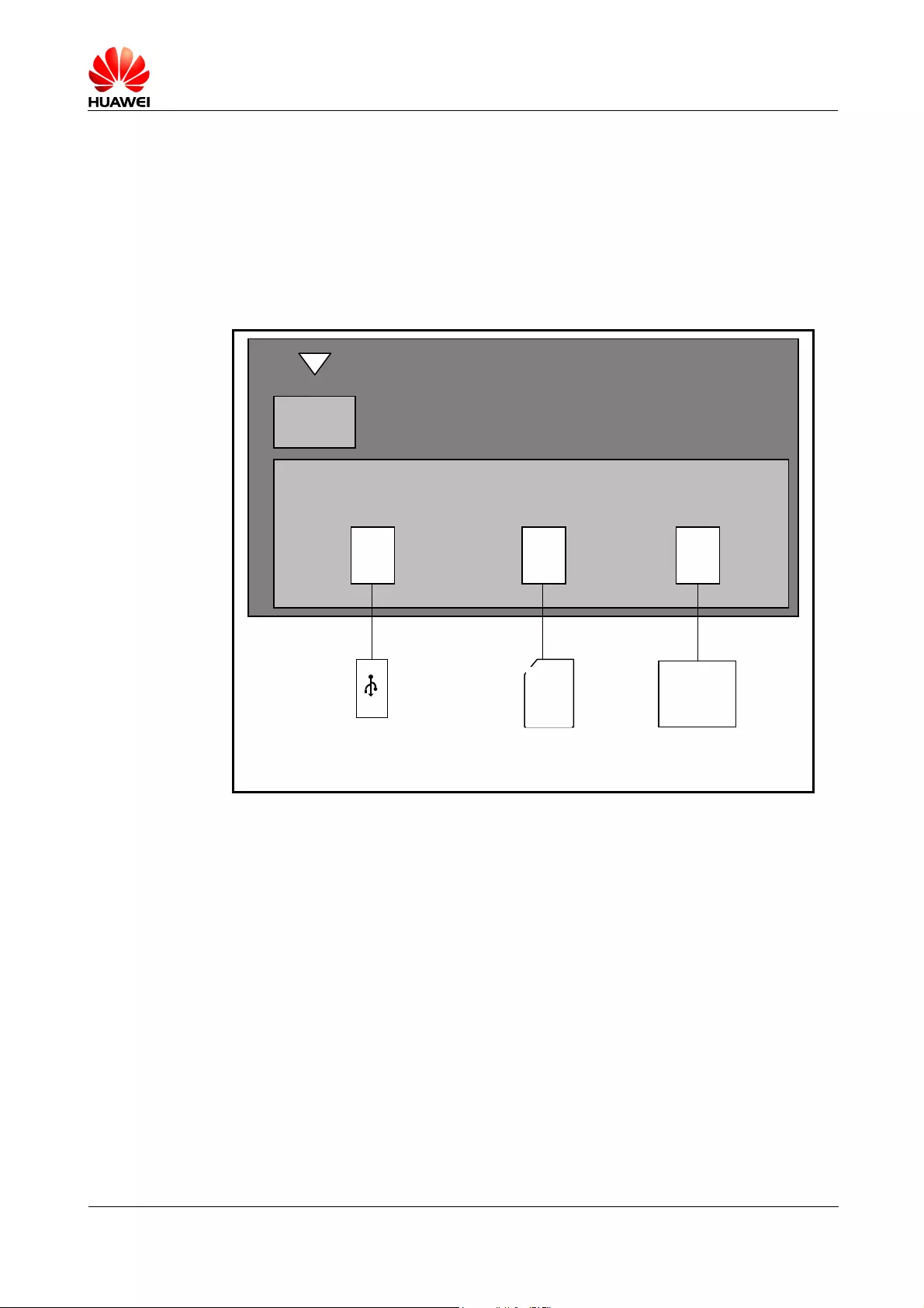
3.4 Circuit Diagram
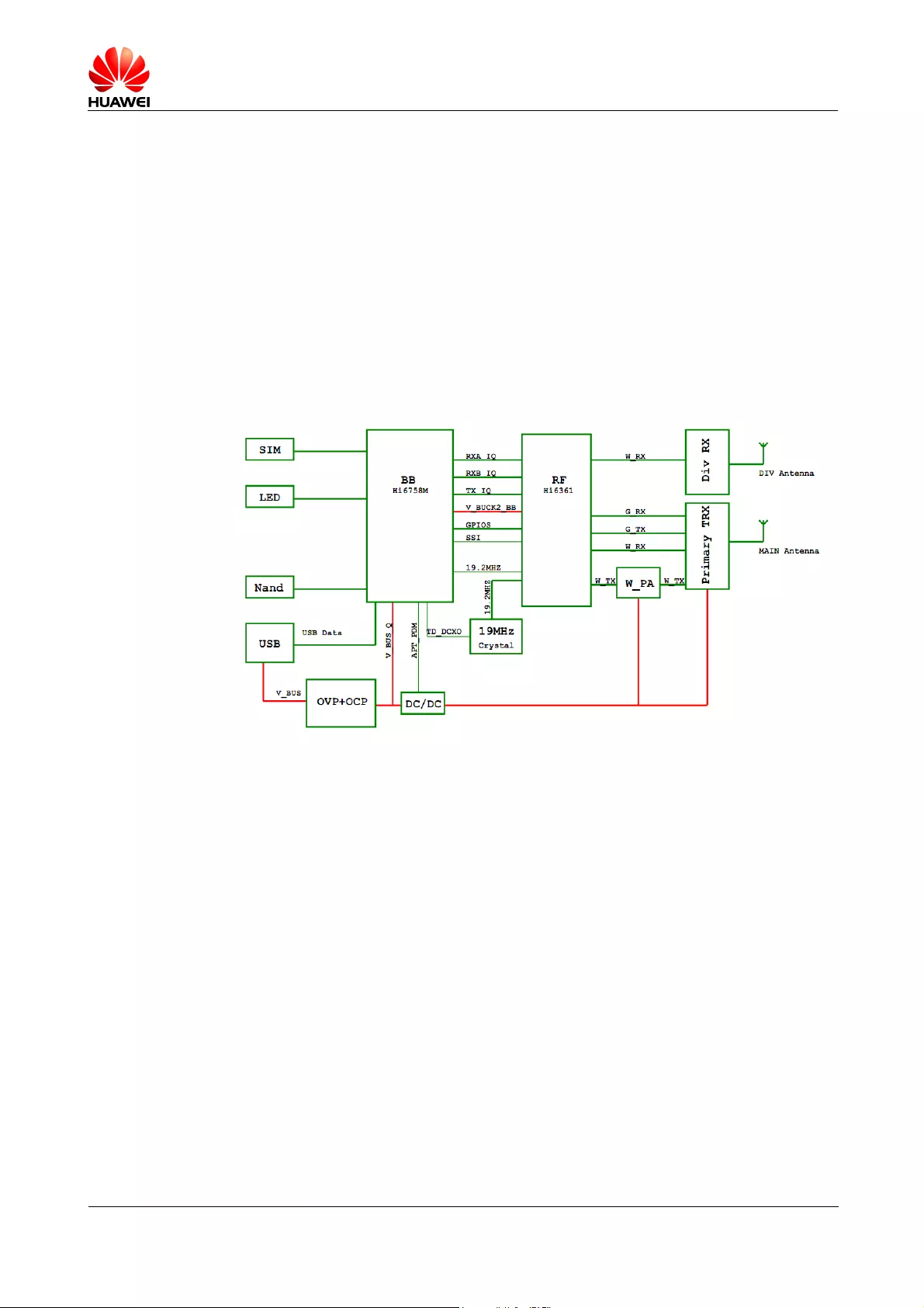
The MS2131 contains the following functional modules, as shown in Figure 3-1.
Baseband processor (BB) and RF processor (RTR)
Nand flash
19.2 MHz crystal resonator
RF c ircuit
Antenna
USB2.0 port
Figure 3-1 MS2131function block diagram
MS2131
Hardware Design Guide
MS2131 Overall Description
Issue 02 (2017-1-13) Huawei Proprietary and Confidential
Copyright © Huawei Technologies Co., Ltd.
11
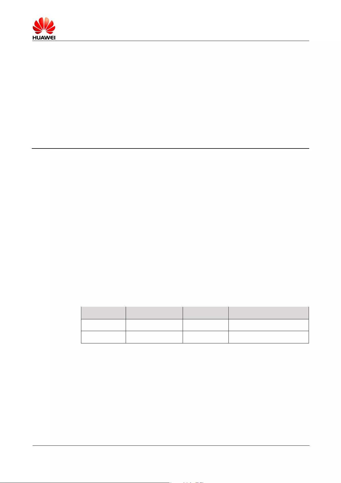
3.5 Port Application Diagram
The MS2131 contains the following ports, as shown in Figure 3-2.
USB2.0 port
SIM card slot (1.8 V or 3.0 V)
TS-5 external antenna port
Figure 3-2 MS2131 application diagram
MS2131
Application interfaces
USB SIM TS-5
SIM
card
External
antenna
RF
MS2131
Hardware Design Guide
MS2131 Interface Features and Design Requirements
Issue 02 (2017-1-13) Huawei Proprietary and Confidential
Copyright © Huawei Technologies Co., Ltd.
12
4 MS2131 Interface Features and Design
Requirements
4.1 About This Chapter
This chapter describes the port connector specifications and usage requirements of the
MS2131. Strictly follow the specified design requirements when designing the interface
circuits of a host.
4.2 MS2131 Interface Introduction
4.2.1 USB Port and Reference Circuits
The MS2131 communicates with the host over the USB port, which supports the USB2.0
protocol. The MS2131 has the USB signals adjusted and provides build-out circuits. The host
must be able to perform impedance matching and protection. Figure 4-1 shows the reference
circuits.
Table 4-1 Signals on the USB port
Pin No. Signal Name I/O Description
1 USB_D+ I/O USB differential data signal+
2 USB_D- I/O USB differential data signal-
MS2131
Hardware Design Guide
MS2131 Interface Features and Design Requirements
Issue 02 (2017-1-13) Huawei Proprietary and Confidential
Copyright © Huawei Technologies Co., Ltd.
13
Figure 4-1 USB port reference circuit diagram
The serial impedance of the USB differential data cables depends on the actual situation. Th e USB
cable routing design must strictly follow the USB2.0 protocol requirements. Cable routing must be
differentiated mode. The control impedance must be 90 Ω.
Electro-static discharge (ESD) components must be as close to the USB port as possible. It is
recommended that you use components with a rated reverse working voltage of 5 V and a junction
capacitance less than 10 pF.
4.2.2 Power Port Introduction
Table 4-2 Power pins
Signal
Name
I/O Description Direct Current Features (V)
Minimum
Value
Typical
Value
Maximum
Value
GND P Power ground
VBUS P USB power supply 4.75 5 5.25
The working power of the MS2131 is provided through the USB port with an input voltage
range from 4.75 V to 5.25 V (typical value: 5 V). Ensure that the power pins are properly
connected during the use of the MS2131 as to maintain its normal performance.
When the MS2131 is dedicated for different applications, attach importance to the power
supply design. In some network environments, when the MS2131works at its largest power
capacity (for example, when it works in GSM mode, a USB voltage dip may occur. Therefore,
make sure the power supply voltage for the host is 3.5 V at the minimum. Otherwise, the
MS2131 may restart.
External power supplies with the current output capacity larger than 2 A are recommended
and that a capacitor of larger than 300 μF and a decoupling capacitor of 0.1 μF must be
paralleled at the power port of the host. When the MS2131 works in GSM mode, its peak
current can reach 2 A. To prevent the MS2131's voltage from dropping to lower than 3.5 V
and help ensure the MS2131 function properly, place a large-capacity capacitor (at least 300
μF) near the USB port.
If the host is powered by batteries, configure a control switching diode or current limiting
chip between the battery power and the MS2131 power port. If a DC/DC converter or

MS2131
Hardware Design Guide
MS2131 Interface Features and Design Requirements
Issue 02 (2017-1-13) Huawei Proprietary and Confidential
Copyright © Huawei Technologies Co., Ltd.
14
low-dropout regulator (LDO) is used for the power supply, the transient current capacity must
be considered.
4.3 SIM Card Port Introduction
A standard SIM card port is embedded in the MS2131. The port supports the 3.0 V and 1.8 V
SIM cards. No external design is required.
MS2131
Hardware Design Guide
MS2131 RF Features and Design Requirements
Issue 02 (2017-1-13) Huawei Proprietary and Confidential
Copyright © Huawei Technologies Co., Ltd.
15
5 MS2131 RF Features and Design
Requirements
5.1 About This Chapter
This chapter describes the MS2131's RF parameters, such as its working bands and wire less
performance specifications, to help you understand the basic MS2131 RF features. As the
design of the host imposes a great impact on the MS2131's wireless performance, this chapter
provides detailed requirements for the host layout and stacking design. The antenna test
environment is also introduced to help you understand the wireless performance test methods
for the MS2131.
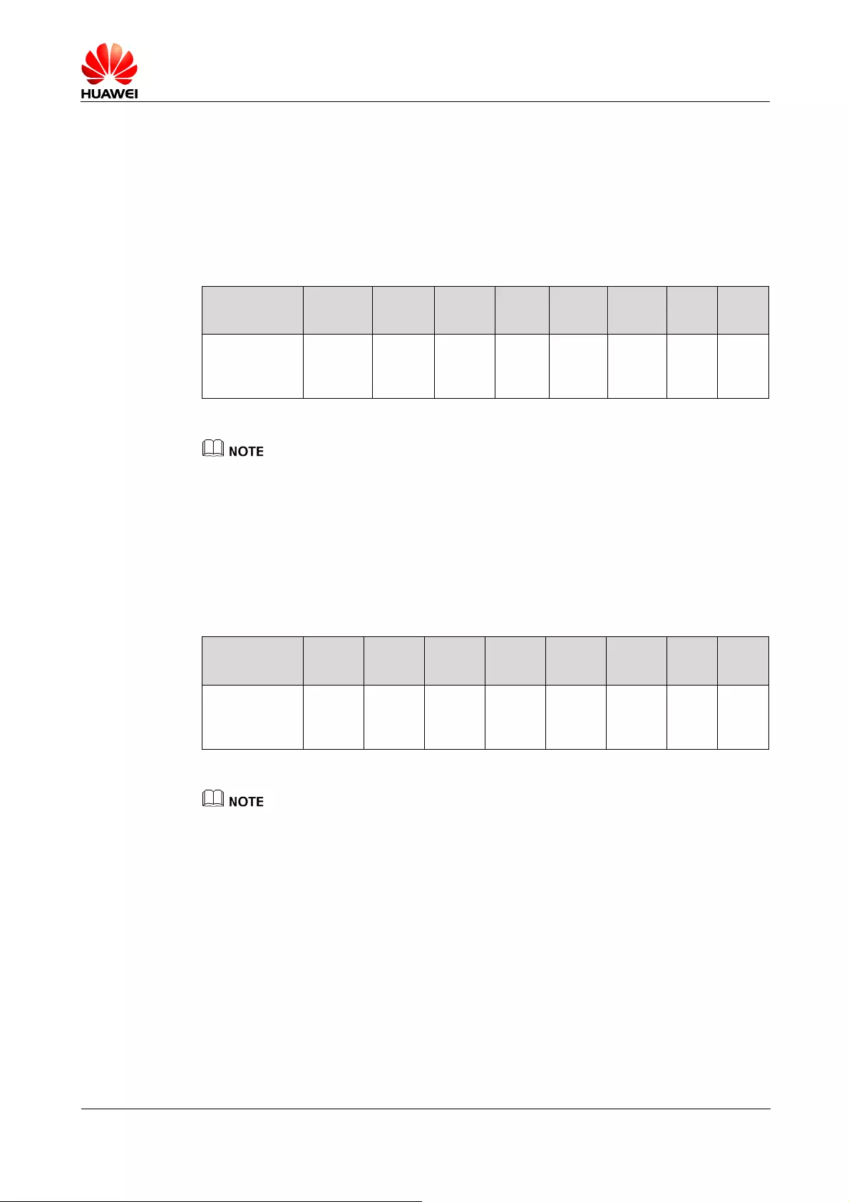
5.2 Working Bands
Table 5-1 describes the working bands that the MS2131 supports.
Table 5-1 MS2131 working bands
Working Band Tx Rx
UMTS Band I 1920–1980 MHz 2110–2170 MHz
UMTS Band II 1850–1910 MHz 1930–1990 MHz
UMTS Band V 824–849 MHz 869–894 MHz
UMTS Band VIII 880–915 MHz 925–960 MHz
GSM1900 1850–1910 MHz 1930–1990 MHz
GSM1800 1710–1785 MHz 1805–1880 MHz
GSM 900 880–915 MHz 925–960 MHz
GSM 850 824–849 MHz 869–894 MHz
MS2131
Hardware Design Guide
MS2131 RF Features and Design Requirements
Issue 02 (2017-1-13) Huawei Proprietary and Confidential
Copyright © Huawei Technologies Co., Ltd.
16
5.3 Wireless Performance Specifications
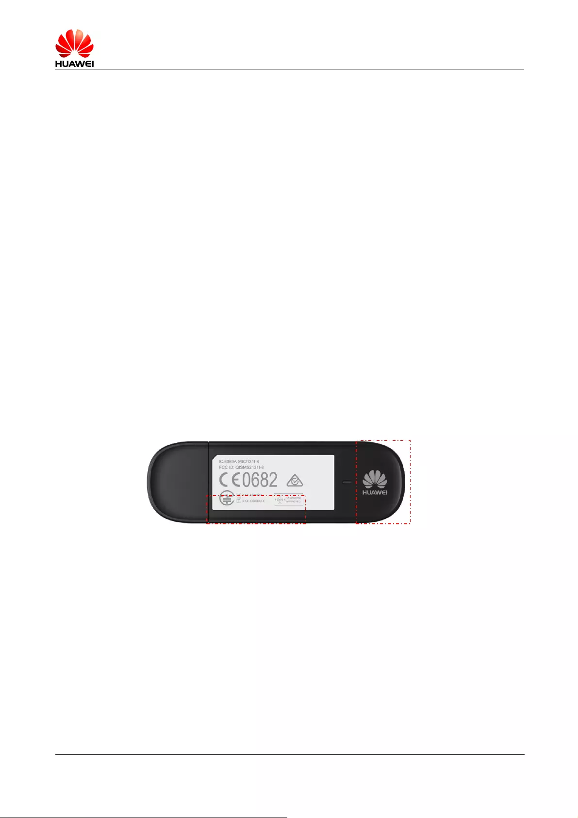
5.3.1 TIS
Total Isotropic Sensitivity (TIS) is an important specification that determines the MS2131's
receiving performance. Table 5-2 describes the TIS specifications of the MS2131.
Table 5-2 MS2131 TIS specifications
Frequency
Band W2100 W1900 W900 W850 G1900 G1800 G900 G850
TIS
specification
(dBm)
–103 –101.5 –100 –98.5 –98.5 –100 –100 –98.5
The preceding design specifications can be realized only when the MS2131 is in optimal layout with
comprehensive shielding measures. Strictly follow the antenna design and stacking requirements to help
realize the optimal MS2131 performance.
5.3.2 TRP
Total Radiated Power (TRP) is an important transmission performance specification of the
MS2131. Table 5-3 describes the optimal TRP specifications of the MS2131.
Table 5-3 MS2131 TRP specifications
Frequency
Band W2100 W1900 W900 W850 G1900 G1800 G900 G850
TRP
specification
(dBm)
18 16.5 18 16.5 22.5 24 27 25.5
The preceding TRP specifications can be realized only when the MS2131 is in optimal layout. Therefore,
strictly follow the antenna design and stacking requirements to help realize the optimal MS2131
performance.
5.4 Antenna Design Requirements
The MS2131 has its antennas embedded and therefore, you do not need to design the antenna.
To ensure the MS2131 antenna performance, the following layout requirements shall be met:
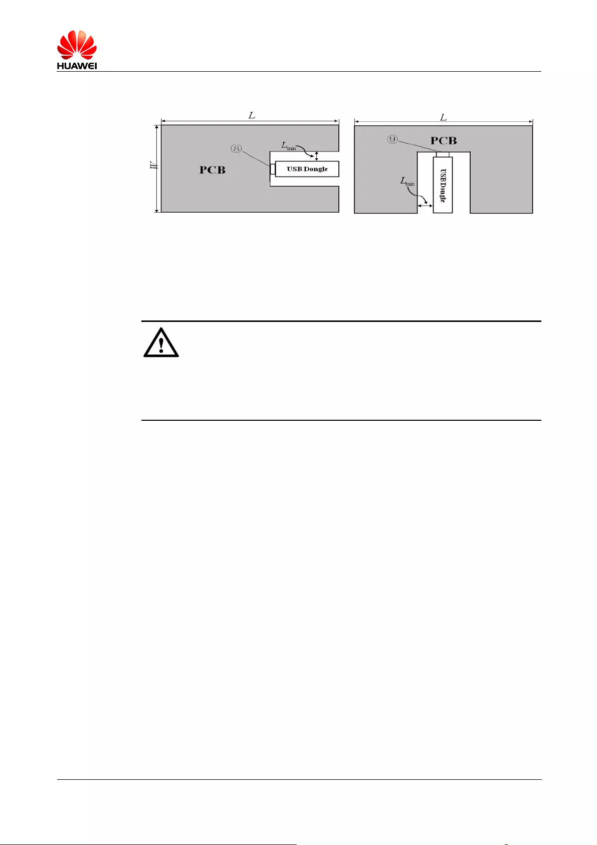
1. The USB dongle be connected to a PCB that has a dimension not less than 10 cm x 10
cm (L x W) (as ① in Figure 5-2). The larger the PCB, the better the antenna
performance can be.
2. If the PCB is approximately a square, the layout shown in Figure 5-2 (excluding the ②
part) be adopted. The USB dongle is placed in the upper or lower part of the PCB side
MS2131
Hardware Design Guide
MS2131 RF Features and Design Requirements
Issue 02 (2017-1-13) Huawei Proprietary and Confidential
Copyright © Huawei Technologies Co., Ltd.
17
(as ③ in Figure 5-2). It is not recommended that the USB dongle be placed in the middle
of the PCB (as ⑧ and ⑨ in Figure 5-4).
3. The USB socket must be properly grounded to the PCB to ensure the optimal antenna
performance. It is not recommended that the PCB extend to the side of the USB dongle.
If this is required (as ② in Figure 5-2), reserve a minimum distance of 5 mm between the
USB dongle and the PCB.
4. Ensure that the USB dongle is in an open area without any other metals shielding around
(such as an earpiece or loudspeaker), except for cases of recommended layouts. If metals
cannot be avoided, a distance larger than 2 cm is required between the USB dongle and
the metal.
5. If there are other antennas in auxiliary devices, the antennas must keep a distance from
the USB dongle to avoid coupling.
6. If the diversity antenna (as ④ in Figure 5-2) is in one side of the USB dongle, the
clearance opening should be faced outwards (as shown in Figure 5-2) to ensure the
optimal antenna performance.
7. In order to minimize devices' impact to the USB dongle, corollary equipment must be
filtered or shielded
8. Do not place any components that adversely affect the antenna performance on the top of
the USB dongle, especially of the main antenna (as ⑤ in Figure 5-2). The antenna
performance will decrease by at least 1.5 dB if any adverse effect occurs.
9. It do not place any metal components around the antenna. Reference Figure 5-3.
Follow the preceding requirements to ensure the optimal MS2131 performance. If any
discrepancy exists, the MS2131 may fail to connect to the network or provide data, voice, or
SMS services.
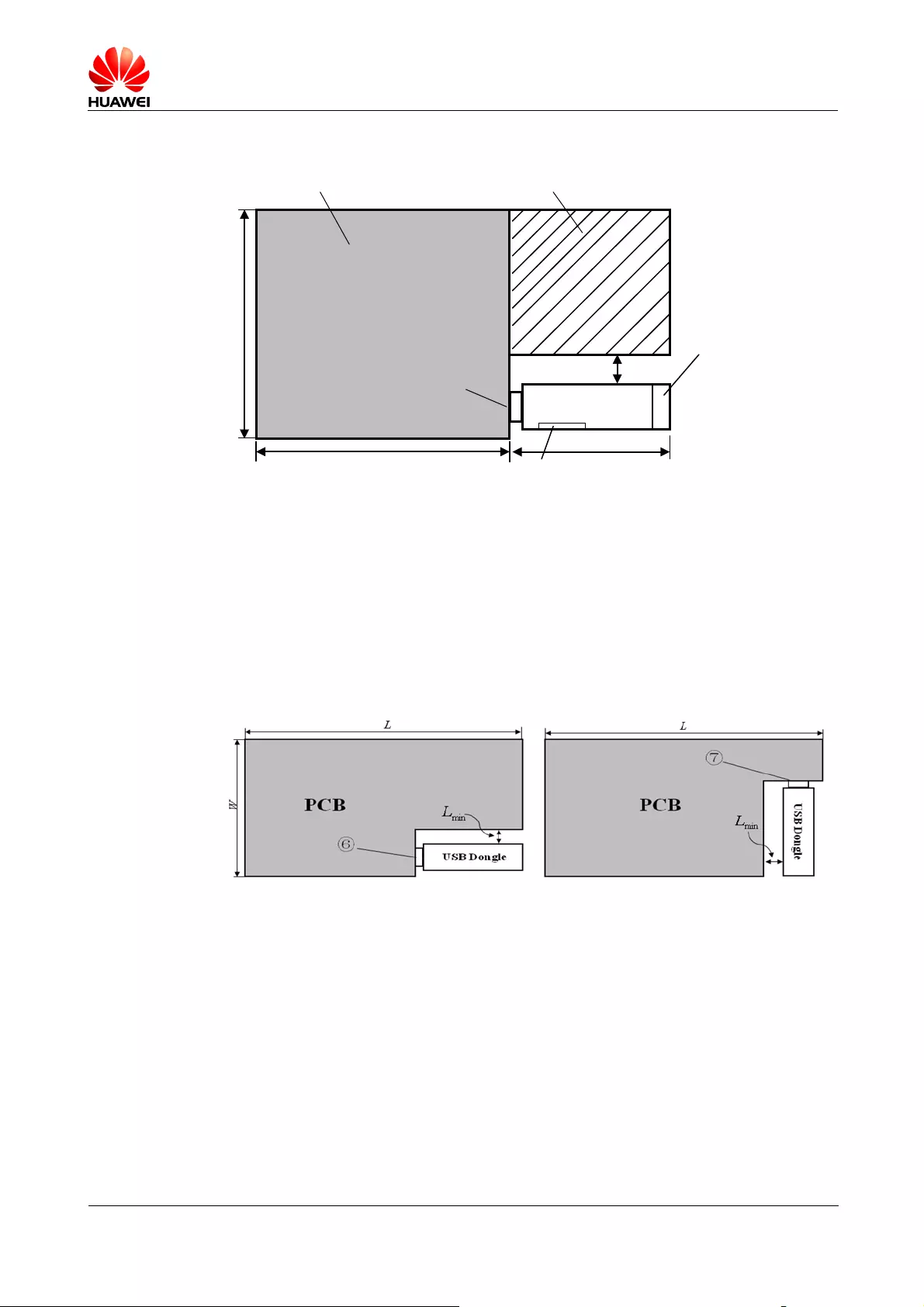
Figure 5-1 MS2131 antenna area
Main
antenna
Diversity antenna
MS2131
Hardware Design Guide
MS2131 RF Features and Design Requirements
Issue 02 (2017-1-13) Huawei Proprietary and Confidential
Copyright © Huawei Technologies Co., Ltd.
18
Figure 5-2 Recommended peripheral layout for the MS2131
Figure 5-3 Two common PCB layouts
Layout 1: The USB dongle is embedded in the longer edge of the PCB. Layout 2: The USB dongle is embedded in the shorter edge of the PCB.
If the terminal device is a rectangle (such as a POS device), the layouts shown in Figure 5-3
are recommended.
1
L
min
L
①
②
③
④
⑤
MS2131
Hardware Design Guide
MS2131 RF Features and Design Requirements
Issue 02 (2017-1-13) Huawei Proprietary and Confidential
Copyright © Huawei Technologies Co., Ltd.
19
Figure 5-4 Two incorrect layouts
Layout 1: The USB dongle is embedded in the middle of the shorter edge.Layout 2: The USB dongle is embedded in the middle of the longer edge.
Figure 5-4 shows two incorrect layouts with the USB dongle embedded in the middle of the
PCB. The omni-directivity of the antenna deteriorates and the efficiency decreases due to the
closed space where the antennas are.
Strictly follow the antenna layout requirements and the stacking requirements specified in
section 6.3.2 "MS2131 Peripheral Staking Requirements" when designing the system. If you
fail to follow the requirements, the TRP and TIS specifications of the MS2131 will deteriorate,
and exceptions, such as network access failures and call failures, will occur.
5.5 Antenna Test Environment
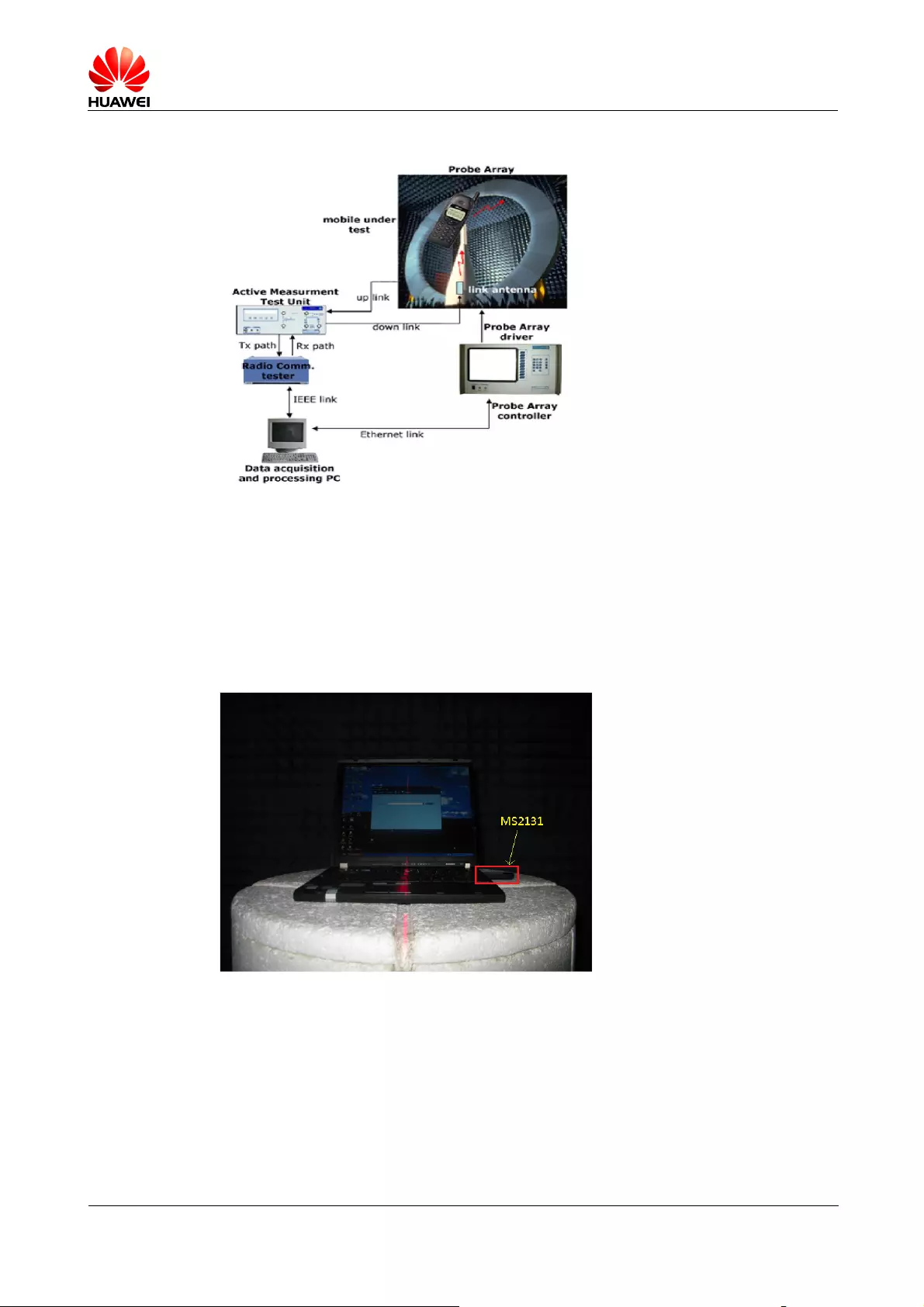
The tests of antenna efficiency, gain, radiation pattern, and TRP and TIS specifications can be
performed in a microwave testing chamber. The following describes the test items in detail:
Passive tests:
− Antenna efficiency
− Antenna gain
− Antenna radiation pattern
− Envelope correlation coeffic ient
Active tests:
− TRP: GSM and WCDMATIS: GSM and WCDMA
CAUTION
MS2131
Hardware Design Guide
MS2131 RF Features and Design Requirements
Issue 02 (2017-1-13) Huawei Proprietary and Confidential
Copyright © Huawei Technologies Co., Ltd.
20
Figure 5-5 SATIMO microwave testing chamber system
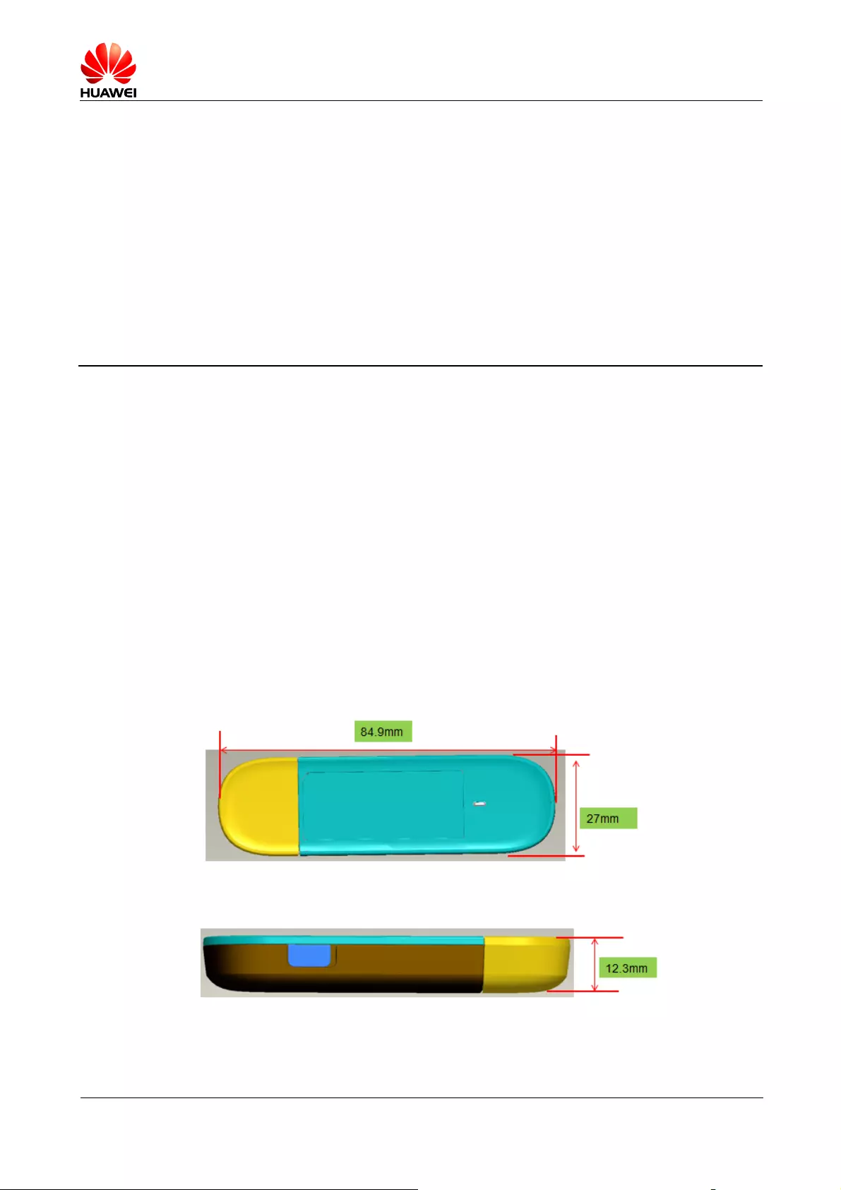
− Auxiliary dedicated test platform:
Design the MS2131 dedicated test platform based on the stacking layout in Figure 5-2. Figure
5-6 shows the platform where a Thinkpad T61 is used. This dedicated platform simulates the
actual system layout to the maximum extent and all the tests and commissioning on the
MS2131 are performed in the platform.
Figure 5-6 Dedicated test platform
MS2131
Hardware Design Guide
MS2131 Structure Features and Design Requirements
Issue 02 (2017-1-13) Huawei Proprietary and Confidential
Copyright © Huawei Technologies Co., Ltd.
21
6 MS2131 Structure Features and Design
Requirements
6.1 About This Chapter
This chapter describes the MS2131 structure features, including the system dimensions and
design requirements addressing the host structure. This chapter also describes the USB
connector dimensions and its design requirements and guides addressing the host structure.
6.2 Dimensions and Weight
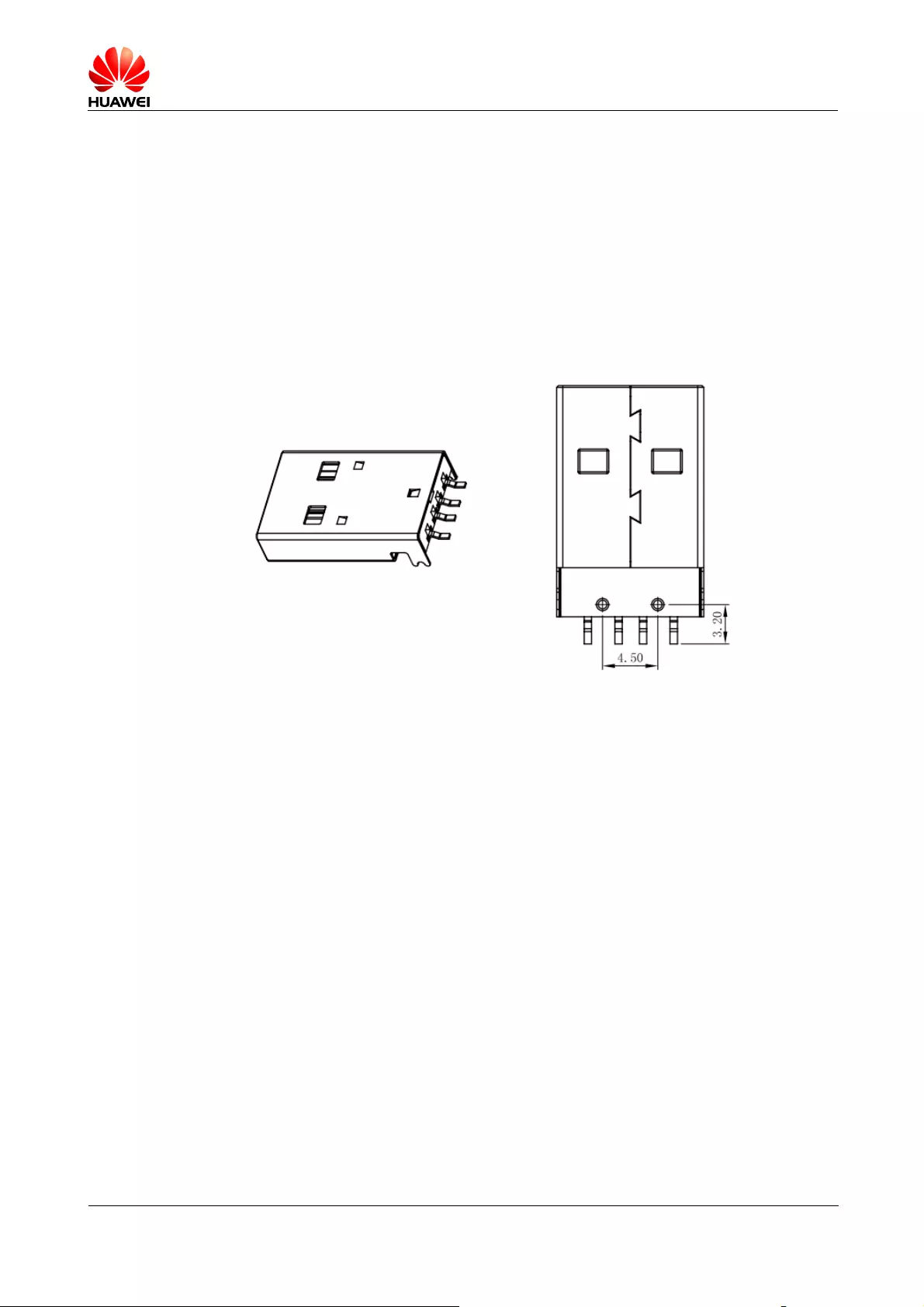
The MS2131 has dimensions of 84.9 mm x 27 mm x 12.3 mm (including the USB cap) and
weighs about 30.0 g.
Figure 6-1 shows the outline dimensions of the MS2131.
Figure 6-1 MS2131 dimensions
MS2131
Hardware Design Guide
MS2131 Structure Features and Design Requirements
Issue 02 (2017-1-13) Huawei Proprietary and Confidential
Copyright © Huawei Technologies Co., Ltd.
22
6.3 MS2131 Design Requirements Addressing the Host
Structure
6.3.1 USB Connector Outline Dimensions
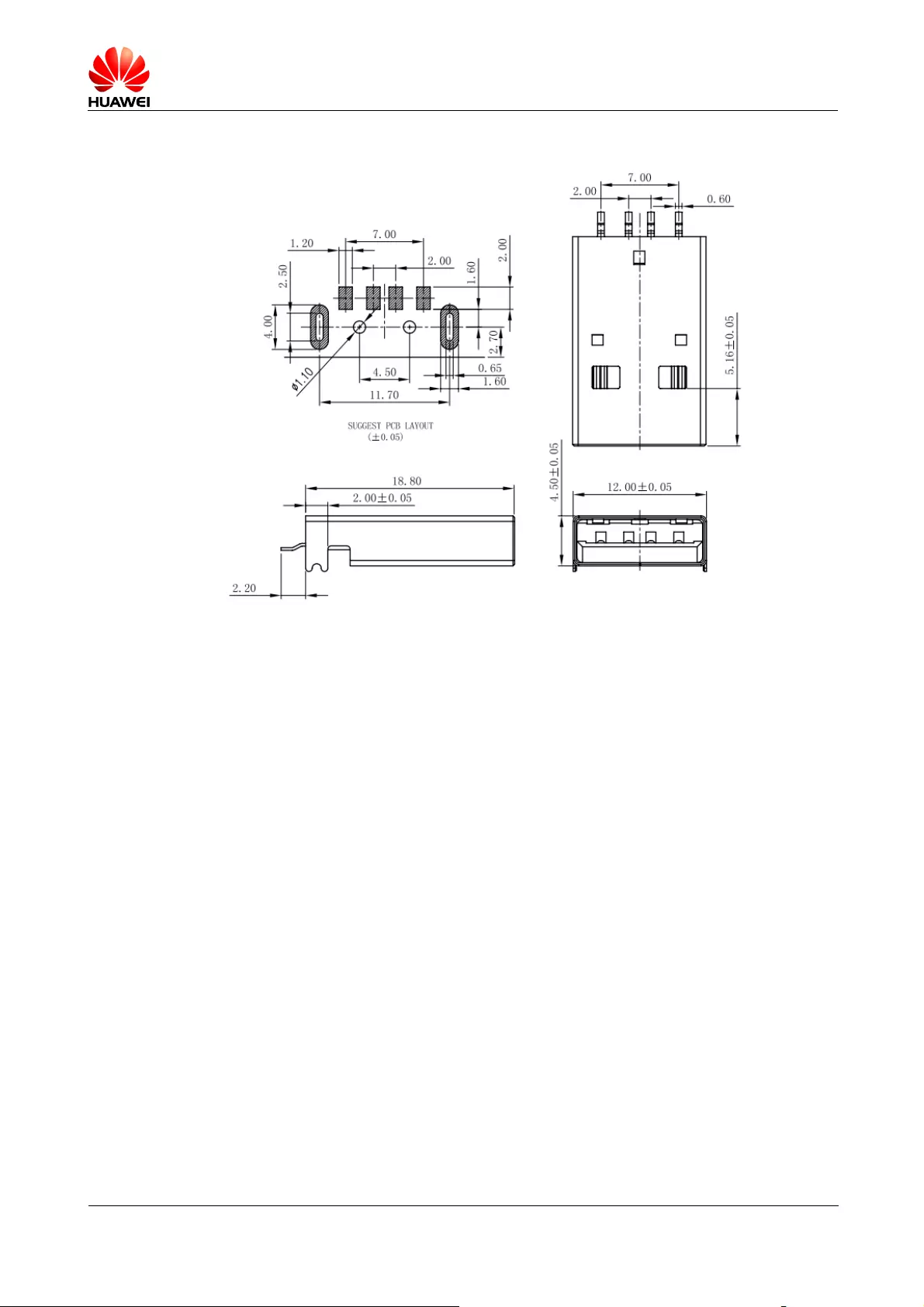
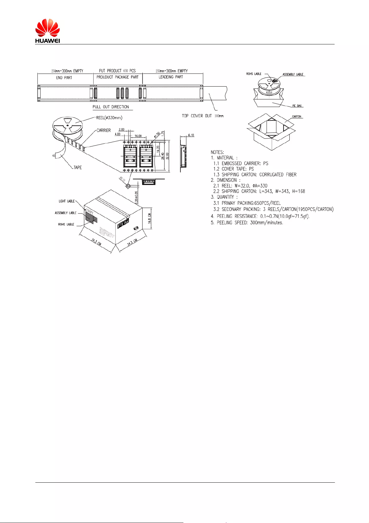
A standard USB2.0 connector, shown in Figure 6-2, is used for the MS2131. The thickness of
the PCB where the connector is inserted must range from 0.6 mm to 1.0 mm. The
recommended thickness is 0.8 mm.
Figure 6-2 USB connector for the MS2131
MS2131
Hardware Design Guide
MS2131 Structure Features and Design Requirements
Issue 02 (2017-1-13) Huawei Proprietary and Confidential
Copyright © Huawei Technologies Co., Ltd.
24
Figure 6-4 Package of the MS2131 USB connector (unit: mm)
6.3.2 MS2131 Peripheral Staking Requirements
When the MS2131 is used in conjunction with the other device,the customer must complete
the design in accordance with the following rules,otherwise it will affect the wireless
performance of MS2131. Detailed rules as follows:
·The customer should be according to the requirements of antenna in section 5.4 to
complete the design firstly,when the MS2131 is used with other device.
·The USB interface between other device and the MS2131,the D+/D- digital line and
VBUS line must be routed at inner layer and packaged with the ground.
·It recommended that the LC parallel resonant network should be reserved at the D+/D-
digital line of the USB interface which is between other device and MS2131 to reduce the
influence of harmonics on low frequency.
·It recommended that the two sides of the component of the interface should leakage of
copper on the PCB surface.
·It recommended that the other high speed communication interfaces such as other USB
interface, SIDO, PCIE, MIPI and so on must be routed at inner layer and packaged with the
ground, and the component of the interface should be shielded,also we suggest the
component of the interface keep 10mm away from the side of the MS2131.

MS2131
Hardware Design Guide
MS2131 Structure Features and Design Requirements
Issue 02 (2017-1-13) Huawei Proprietary and Confidential
Copyright © Huawei Technologies Co., Ltd.
25
·If there are some digital storage unit, such as SIM card, SD card, Flash and so on, these
components and the Peripheral device must be shielded,and keep 10mm away from the side
of the MS2131.
·If there are some Communication FPC boards,such as the LCD,the Touch,the MIC,
and the SPK+, the FPC board suggest doing EMI processing,and the FPC cables should not
be placed near the MS2131.
·If there are some fast switching circuit, such as DCDC circuit, PMU power management
circuit, and other circuit that can produce a large electric current ,they must be shielded, and
keep 10mm away from the side of the MS2131.
·If there are some clock circuit, such as the TCXO circuit,they must be shielded, and
keep 10mm away from the side of the MS2131.
·If there are other baseband signal processing circuit or control circuit, they must be
shielded,and keep 10mm away from the side of the MS2131.
·If there are other RF communication unit, such as WIFI,BT, GPS,NFC and so on, they
must be shielded, and keep 10mm away from the side of the MS2131.
·Some test points for high speed digital signal should be placed far away from the MS2131
about 5mm.
In addition, other components or circuit which can produce strong EMI should be shie lded
and placed far away from the MS2131.
We have given some design rules above for customers to solve the strong interference. If the customers
are unable to meet the design rules, it may decrease the MS2131 performance even the MS2131 cannot
work normally.

MS2131
Hardware Design Guide
MS2131 Power Design Guide
Issue 02 (2017-1-13) Huawei Proprietary and Confidential
Copyright © Huawei Technologies Co., Ltd.
26
7 MS2131 Power Design Guide
7.1 About This Chapter
This chapter describes the MS2131's power features and power supply requirements in
different scenarios and its power consumption data in sleep mode. For details about the power
supply circuit over which the host powers an embedded MS2131, see section 7.6 "Peripheral
Power Design Requirements."
7.2 MS2131 Power Supply
The working power of the MS2131 is provided through the USB port with an input voltage
ranging from 4.75 V to 5.25 V (typical value: 5 V).
7.3 MS2131 Power Requirements in 2G Mode
This section describes the MS2131 power features when in use in 2G mode. The power
consumption of the MS2131 increases with its transmit power. Transmit power, also called
uplink power, is the amount of power used during transmission from a wireless terminal to a
base station.
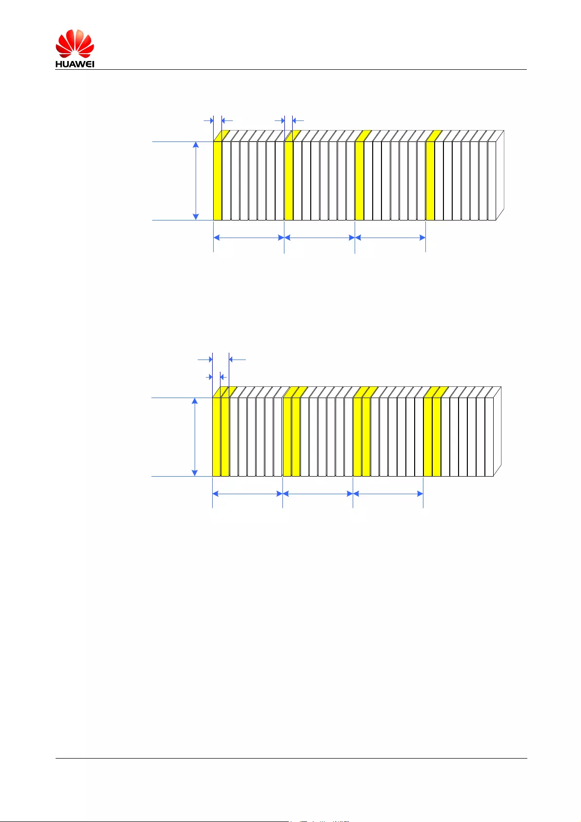
The Time Division Multiple Access (TDMA) uses GSM as the access method, and therefore,
the MS2131 transmits signals only in slots specified by the base station. Each GSM
transmission cycle has eight slots, 577 µs each. The MS2131 transmits power in one out of
the eight slots. As calculated, each GSM transmission cycle lasts 4.61 ms and the transmission
duration lasts 577 µs. This transmission mode is called "burst". The better signal reception
quality is, the less power consumption of the MS2131 will produce, and vice versa. The
maximum power consumption is 33 dBm (GSM900).
Figure 7-1 shows the GSM working principle.
MS2131
Hardware Design Guide
MS2131 Power Design Guide
Issue 02 (2017-1-13) Huawei Proprietary and Confidential
Copyright © Huawei Technologies Co., Ltd.
27
Figure 7-1 GSM working principle
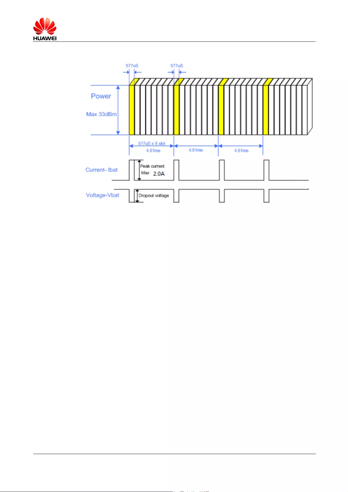
For GPRS mode, the uplink transmission occurs in two or more than two continuous slots, as
shown in Figure 7-2.
Figure 7-2 GPRS working principle
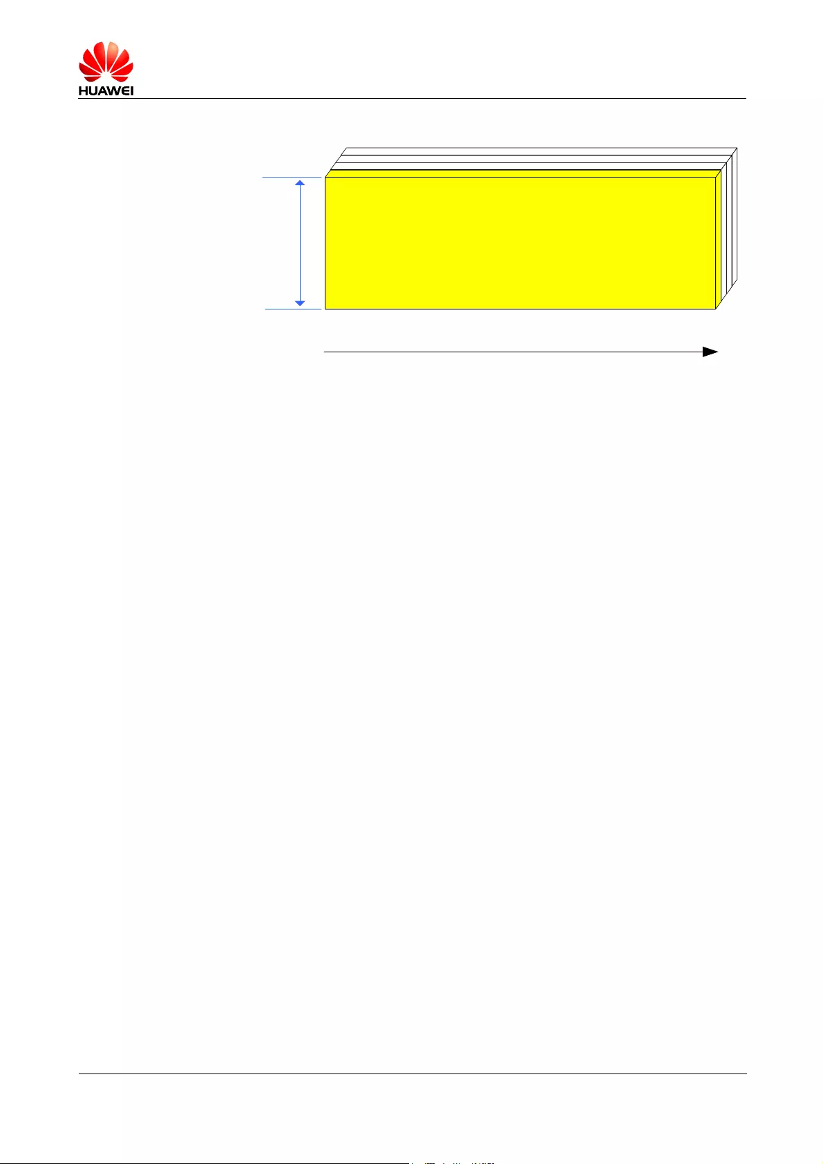
In GSM mode, the MS2131 power transmission occurs in cycles and has transient changes
during each transmission, as shown in Figure 7-3.
577uS 577uS
577uS x 8 slot
4.61ms 4.61ms 4.61ms
Power
Max 33dBm
577uS
577uS x 8 slot
4.61ms 4.61ms 4.61ms
Power
1.15ms
Max 30dBm
MS2131
Hardware Design Guide
MS2131 Power Design Guide
Issue 02 (2017-1-13) Huawei Proprietary and Confidential
Copyright © Huawei Technologies Co., Ltd.
28
Figure 7-3 Transient power changes
Seen from Figure 7-3, the GMS power amplifier (PA) performs the transmission in the
transmission slots. In case of poor signal reception, the PA transmission power may reach 33
dBm. The transient MS2131 power supply current may reach 2 A and a voltage drop then
occurs.
The following are two reasons accounting for the MS2131 power supply voltage drop:
The transient response function of the power supply cannot meet the requirement for the
2 A transient output within several microseconds.
There is output impedance at the MS2131 power connector, and the currents are large.
When the transmission slot ends, the GSM PA shuts down, the power supply current then
drops, and the voltage resumes. After 4.651 ms, another transmission slot comes, causing a
voltage drop again.
Therefore, the MS2131 operating in 2G mode must have good transient response performance
and small internal resistance to prevent voltage drop. Considering the product cost and that
the MS2131 can operate within a certain range of voltages, the minimum voltage of the power
supply is 3.5 V.
7.4 MS2131 Power Requirements in 3G Mode
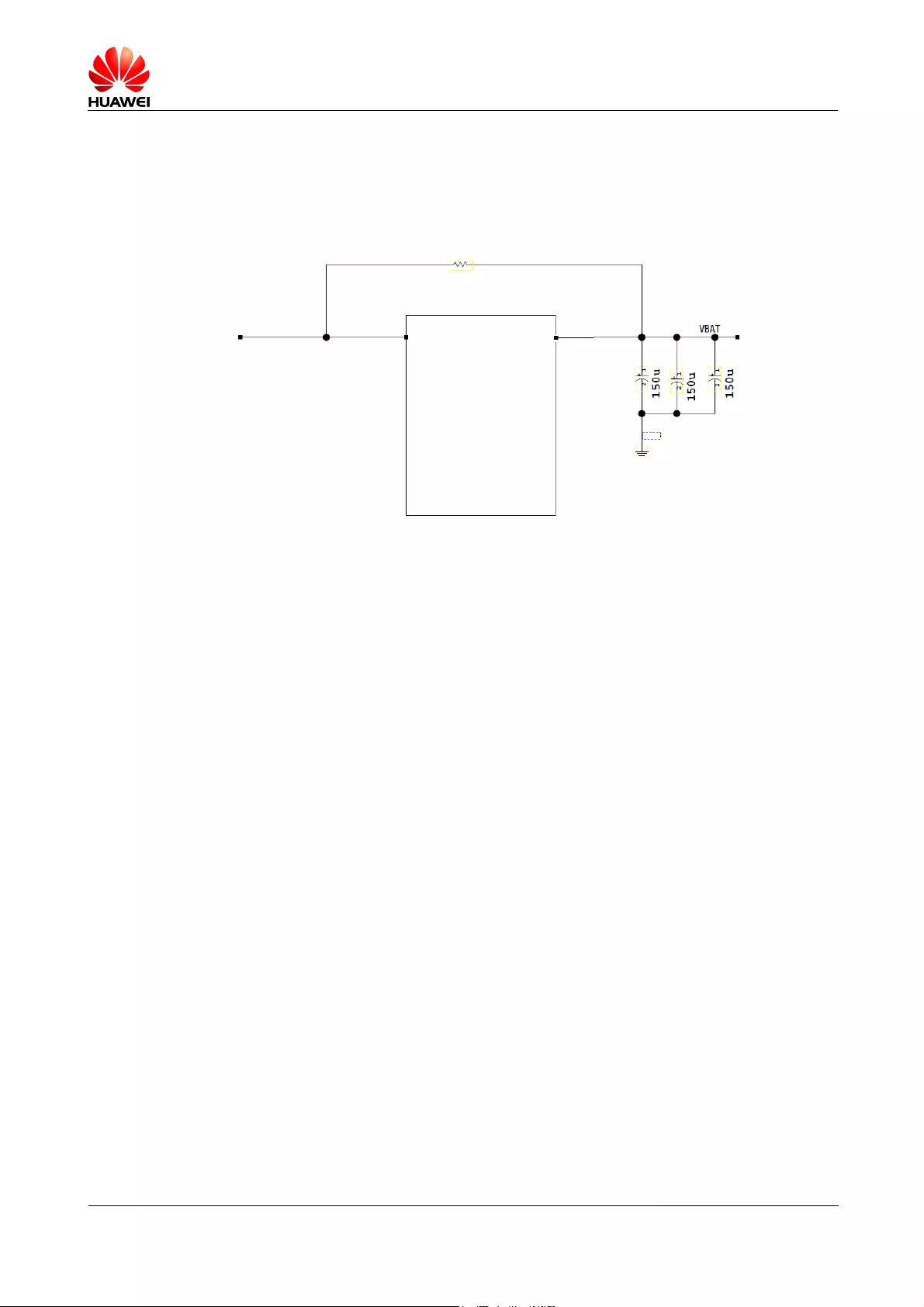
In a 3G network, no correlation exists between the transmission power and time.
Figure 7-4 shows the transmission power in a 3G network.
MS2131
Hardware Design Guide
MS2131 Power Design Guide
Issue 02 (2017-1-13) Huawei Proprietary and Confidential
Copyright © Huawei Technologies Co., Ltd.
29
Figure 7-4 3G network transmission
7.5 MS2131 Power Consumption Features
The maximum transmission power capacity for a wireless terminal in a 3G network is 24 dBm
while the maximum transient power supply current is about 2 A. Therefore, a minimum
current output capacity of 800 mA at average is required to satisfy the load requirements. The
following specifications are for reference only:
Power consumption in a 3G network with a 7.2 Mbps download speed and an RF power
capacity of 10 dB: 5 V and less than 250 mA
Power consumption in a 3G network with a 2 Mbps download speed and an RF power
capacity of 22 dB: 5 V and less than 500 mA
Power consumption in standby mode with a 3G network connected: 5 V and less than 100 mA
7.6 Peripheral Power Design Requirements
Power supplied to the MS2131 must have a minimum general current of 800 mA and a
minimum transient current of 2 A. The peripheral power design must be dedicated to these
requirements, to help the MS2131 bear the power supply voltage drop for transmission in
GSM mode.
To address the voltage drop, the following requirements must be met for peripheral power
design:
Reducing the peripheral power impedance (including the power cable routing to the
MS2131)
Adding energy storage capacitors
Using the dynamic response function of power module chips
7.6.1 Recommended Power Supply Structure
A power structure of a DC-DC output, power supply over a switching diode, and a current
limiting circuit is recommended. The host can then be enabled to control the MS2131 power
time
Power
Max 24dBm
MS2131
Hardware Design Guide
MS2131 Power Design Guide
Issue 02 (2017-1-13) Huawei Proprietary and Confidential
Copyright © Huawei Technologies Co., Ltd.
30
switch and disconnect the power to the MS2131 when exceptions occur. The DC impedance
of the current limiting circuit or switching diode must be less than 50 mΩ. To avoid an
oversize impedance, reserve space for a 0 Ω resistor for compatible purpose.
Figure 7-5 Recommended power structure
Compatible with a 0 ohm resistor
Current limiting chip or
power control circuit
7.6.2 Derating Requirements
It is recommended that an 85% derating capacity be provided for the external power supply
voltage and current. If a DC/DC converter or LDO is used, ensure its derating capacity and
transient conductivity.
7.6.3 Peripheral Power Supply Design Rules
The peripheral power supply design rules for the MS2131 are described as follows:
1. The power cable routing path must be as wide as possible to bear currents larger than 2
A during transmission in GSM mode.
2. A large-capacity capacitor (at least 300 uF) must be placed near the USB port to prevent
its voltage from dropping lower than 3.5 V. Energy storage capacitors used for must be
placed near the MS2131 as much as possible to ensure optimal discharge performance of
the capacitors.
3. Overvoltage and anti-reversion diodes must be connected to external power supply
connectors to protect the power circuits when exceptions occur.
4. If the host supplies power to the MS2131 over a DC/DC converter, the converter must be
able to bear the 2 A transient current.
5. The USB power cable voltage fluctuates in GSM mode. Therefore, do not route sensitive
signal cables near the USB power cable.

MS2131
Hardware Design Guide
MS2131 PCB Design Guide
Issue 02 (2017-1-13) Huawei Proprietary and Confidential
Copyright © Huawei Technologies Co., Ltd.
31
8 MS2131 PCB Design Guide
This chapter describes the PCB interconnection design requirements and precautions for the
host. Complying with these requirements and following these precautions help ensure the
performance of the MS2131 when interconnected with the host and reduce user costs.
8.1 General PCB Design Rules
To ensure the signal integrity and conductivity between the MS2131 and its peripherals,
maximize the power cable routing width. Ensure a conductivity of 2 A.
The two surfaces of USB differentiated signal must be surrounded by grounds and the
impedance must be controlled in a proper range. Do not interrupt the signal with strong
interference or sensitive signals.
8.2 Power Design
The power design is a key factor for the MS2131 performance, which has impacts on the
following specifications:
EMC performance
Radio modulation spectrum
Phase and receiving sensitivity
The general power design rules are described as follows:
Ensure a good power quality. Reduce the power ripple for a switched-mode power
supply and noise interference for a linear power supply.
Place the filter capacitors for the power supply as close to the power pins for the USB
connector as possible. Place the capacitor with less capacitance closer to the power pins.
Use capacitors of 150 μF, 4.7 μF, 10 nF, 100 pF, and 33 pF.
Try to minimize the voltage drop caused by the power cable routing and ensure a conductivity
of 2 A.
MS2131
Hardware Design Guide
MS2131 PCB Design Guide
Issue 02 (2017-1-13) Huawei Proprietary and Confidential
Copyright © Huawei Technologies Co., Ltd.
32
8.3 Cable Routing Rules
8.3.1 Power Design
The power consumption of the MS2131 varies by network standard. Working in GSM mode,
the MS2131 has a peak current of larger than 2 A. To ensure a sufficient power capacity and
minimize the voltage drop caused by cable routing, a 100-mil cable routing width is
recommended and the finish copper thickness is 1 OZ. If possible, maximize the power cable
routing width.
8.3.2 USB Signal Cable Routing Design
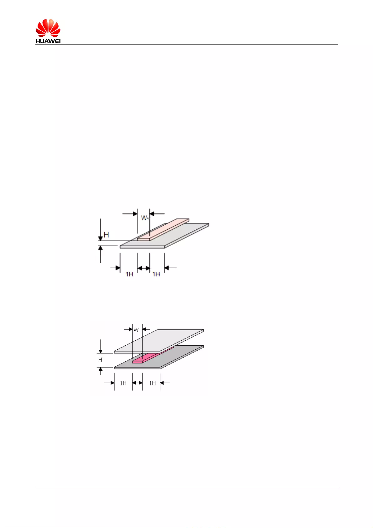
The impedance for the USB signal cable on the user PCB must be 90 Ω. The impedance is
dependent on the dielectric constant, cable width, and the distance from the ground. Figure
8-1 and Figure 8-2 show the structures and stacking designs of the 90 Ω impedance
microstrips and strip lines that can be adopted for the cabling impedance design.
Figure 8-1 Microstrip structure
Figure 8-2 Strip line structure
You can use either of the preceding ways to design the 90 Ω cabling impedance.
Note that the USB signal cabling impedance must be dedicatedly designed and the two sides
of the USB must be fully surrounded by grounds.

MS2131
Hardware Design Guide
MS2131 PCB Design Guide
Issue 02 (2017-1-13) Huawei Proprietary and Confidential
Copyright © Huawei Technologies Co., Ltd.
33
8.3.3 Grounding Measure
To protect the USB signals from interference and sensitive sources, surround the USB
surfaces by grounds.
Ensure the continuity of reference grounds for all signal cables to avoid cross division.
Ensure a minimum loop path for each signal cable.

MS2131
Hardware Design Guide
MS2131 ESD Design Guide
Issue 02 (2017-1-13) Huawei Proprietary and Confidential
Copyright © Huawei Technologies Co., Ltd.
34
9 MS2131 ESD Design Guide
9.1 PCB Design Recommendations for the Host
1. A four-layer or six-layer PCB is recommended. Two-layer PCBs are not recommended.
2. Use a large-capacity ceramic bypass capacitor and decoupling capacitor on the MS2131
power supply. Place the capacitors within 30 mils from the connector. The PCB cable
routing width must be at least 20 mils. Deploy dedicated power cable plane and ground
or tight power and ground grid. Use a transient voltage suppressor (TVS) for external
electrical overstress (EOS) protection. It is recommended that a component that has a
peak power larger than 100 W at 8/20 µs be used.
3. If the signal cable length is larger than 300 mm (12 inches), surround the sides of the
signal cables by grounds. Drill holes on the grounds to connect them to the main ground.
4. When connecting the host to the MS2131, ensure the grounding reliability.
5. Use TVSs at the joint between the MS2131 and the host. The TVS on the male connector
must have a parasitic capacitance less than 1 pF while the TVS on the power supply must
have a peak power larger than 100 W at 8/20 μs
9.2 Shell Design Recommendations for the Host
The MS2131 comes with ESD protection. The SIM card and connector have high
requirements for ESD protection.
To prevent users from directly touching the SIM card area, cover the area with a mechanical
part.

MS2131
Hardware Design Guide
MS2131 Electrical and Reliability Features
Issue 02 (2017-1-13) Huawei Proprietary and Confidential
Copyright © Huawei Technologies Co., Ltd.
35
10 MS2131 Electrical and Reliability
Features
10.1 About This Chapter
This chapter describes the electrical and reliability features of the MS2131 interfaces,
inc luding:
Ultra working conditions
Working and storage environment
Power features
Reliability features
ESD features
10.2 Ultra Working Conditions
Table 10-1 lists the working condition limitation for the MS2131. Permanent damage may be
caused to the MS2131 if used beyond the conditions.
Table 10-1 Ultra working conditions of the MS2131
Symbol Parameter Minimum Value Maximum
Value
Unit
VBUS External power supply –0.3 5.25 V
WARNING
MS2131
Hardware Design Guide
MS2131 Electrical and Reliability Features
Issue 02 (2017-1-13) Huawei Proprietary and Confidential
Copyright © Huawei Technologies Co., Ltd.
36
10.3 Working and Storage Environment
Table 10-2 lists the working and storage environment for the MS2131.
Table 10-2 Working and storage environment for the MS2131
Parameter Minimum Value Maximum
Value
Unit
Normal working temperature –20 55 °C
Storage temperature –40 70 °C
Humidity range 5 95 %
10.4 Power Features
10.4.1 Input Power
Table 10-3 lists the specifications for the MS2131 input power.
Table 10-3 Specifications for the MS2131 input power
Parameter Minimum
Value
Typical
Value
Maximum
Value
Ripple Unit
VBUS 4.75 5 5.25 < 50 mVpp
(0 Hz to 2.5 GHz)
V
10.4.2 Working Current
The MS2131 working current is specified in section 11.1 "Appendix One MS2131 Power
Consumption Data in Different Scenarios", obtained from a test using direct current and
having a typical power supply of 5 V.
10.5 Reliability Features
Table 10-4 describes the MS2131 reliability test conditions and results.
Table 10-4 MS2131 reliability test conditions and results
Test Item Test
Result Test Parameter
1 Drop test in common
temperature PASS 0.8 m for six surfaces

MS2131
Hardware Design Guide
MS2131 Electrical and Reliability Features
Issue 02 (2017-1-13) Huawei Proprietary and Confidential
Copyright © Huawei Technologies Co., Ltd.
37
Test Item Test
Result Test Parameter
2 Weight bearing test PASS 70 kgf for 2s on the front and rear surfaces
3 Pressing test PASS 120 N for the surfaces
4 Bending test PASS 2 kgf for 1min
5 Twisting test PASS 0.5 Nm for 500 times
6 Swapping/disassembling
endurance test PASS Connecting to an antenna for 3000 times
7 Working vibration PASS
Sine wave vibration
1. Frequency range: 5 to 500 Hz
2. Acceleration: 2G
3. Sweep frequency: 0.5 oct/min
4. Test duration: three directions (X, Y, and Z),
2h for each direction
Random Vibration
1. Frequency range: 5 to 500 Hz
2. PSD: 0.04 g²/Hz
3. Test duration: three directions (X, Y, and Z),
1h for each direction
8 Working shock PASS
1. Half sine wave with an acceleration speed of
300 m/s²
2. Pulse duration: 11 ms
3. Shock times: Six directions, three times for
each direction, 18 times in total
9 Low-temperature
storage PASS
–40°C for 24 hours with all specifications,
functions, and mechanical performance
remaining normal
10 High-temperature
storage PASS
85°C for 24 hours with all specifications,
functions, and mechanical performance
remaining normal
11 Low-temperature
operation PASS
–20°C for 24 hours with all RF specifications
and electrical performance remaining normal
(during developing phase)
12 High-temperature
operation PASS
55°C for 24 hours with all RF specifications and
electrical performance remaining normal (during
developing phase)
13 Damp heat cycling PASS
Raise the humidity to 95% within 1h and keep
the test chamber temperature at 25°C. Raise the
temperature to 55°C within 3h and keep the
humidity at 95%. Keep the temperature at 55°C
and the humidity at 95% for 9h. Decrease the
temperature to 25°C within 3h and keep the
humidity at 95%. Keep the test chamber
temperature at 25°C and humidity at 95% for 9h.
The pr
eceding operations are one cycle. Perform
two cycles for the test.

MS2131
Hardware Design Guide
MS2131 Electrical and Reliability Features
Issue 02 (2017-1-13) Huawei Proprietary and Confidential
Copyright © Huawei Technologies Co., Ltd.
38
Test Item Test
Result Test Parameter
14 Temperature shock PASS
Use two chambers. Keep the temperature at
–40°C for one hour and then 70°C for another
hour at a maximum interval of 20 seconds.
Perform 24 cycles for this test.
15 Solar radiation PASS 1120 W/m² for 20h and dark for 4h. Perform
three cycles for the test.
16
Salt fog test PASS Keep the density at 5% for 8h for the entire
system.
17 High temperature and
high humidity PASS
1. Power on the sample. Ensure the sample
functions at a maximum transmit power.
2. Test temperature: 55±1°C
3. Test humidity: 95±2% RH
4. Test duration: 168h
5. Test time point: 48h, 96h, 144h, and 168h
6. Restoration temperature and duration: 25°C
for 2h
18 Temperature cycle test PASS
1. Power on the sample. Ensure the sample
functions at a maximum transmit power.
2. Temperature change ranges: –10±1°C to
+55±1°C
3. Temperature change rate: 10°C/min
4. Number of recycles: 120 cycles, one cycle
including 30min at low temperature and 30min
at high temperature
19 Radiated emission (RE) PASS Frequency range: 30 MHz–6 GHz
Criterion: CISP R22 Class B
20 Conducted emission
(CE) PASS Frequency range: 150 KHz–30 MHz
Criterion:
CISPR22 Class B
21 Radiated spurious
emission (RSE) PASS Frequency range: 30 MHz–12.75 GHz
22 ESD PASS
Interference voltage:
Air discharge: 10 kV; contact discharge 6 kV
Criterion: TT/TR
23 Radiated susceptibility
(RS) PASS
Frequency range: 80 MHz–2.7 GHz. No test is
required for the main working bands.
Interference field strength: 4 V/m (80% AM is
performed)
Criterion: CT/CR

MS2131
Hardware Design Guide
MS2131 Electrical and Reliability Features
Issue 02 (2017-1-13) Huawei Proprietary and Confidential
Copyright © Huawei Technologies Co., Ltd.
39
The MS2131 has dedicated ESD requirements. To ensure the proper connection between the
MS2131 and the user interface board reference ground, it is recommended that copper studs
or other low-impedance metal fasteners be used for the copper exposure (to connect to an
interface reference ground) of the positioning holes on the user interface board.
CAUTION
MS2131
Hardware Design Guide
Appendix
Issue 02 (2017-1-13) Huawei Proprietary and Confidential
Copyright © Huawei Technologies Co., Ltd.
40
11 Appendix
11.1 Appendix One MS2131 Power Consumption Data in
Different Scenarios
Table 11-1 MS2131 working current (5 V) in common scenarios
Description Bands
Current
Units Notes/Configuration
HSDPA/WCDMA
UMTS
bands
50
mA
Power up and idle (DRX cycle = 8
[2.56 sec])
230 mA
Phone call (TX power = 10 dBm)
230
mA
DL Rate = 7.2 Mbps (TX power =
10 dBm)
GSM/GPRS/EDGE
GSM
bands 50
mA
Power up and idle (MFRMS = 5
[1.175 sec])
140 mA
Phone call (TX power = 10 dBm)
Table 11-2 Peak working currents in GPRS mode
Bands Averaged
Current
Peak
Current
Units TX Power TX slot
GPRS 850
230
1640
mA
PCL = 5
1 Up/1 Down
GPRS 900
240
1540
mA
PCL = 5
1 Up/1 Down
GPRS 1800
180
1000
mA
PCL = 2
1 Up/1 Down
GPRS 1900
160 1050 mA
PCL = 0
1 Up/1 Down
MS2131
Hardware Design Guide
Appendix
Issue 02 (2017-1-13) Huawei Proprietary and Confidential
Copyright © Huawei Technologies Co., Ltd.
41
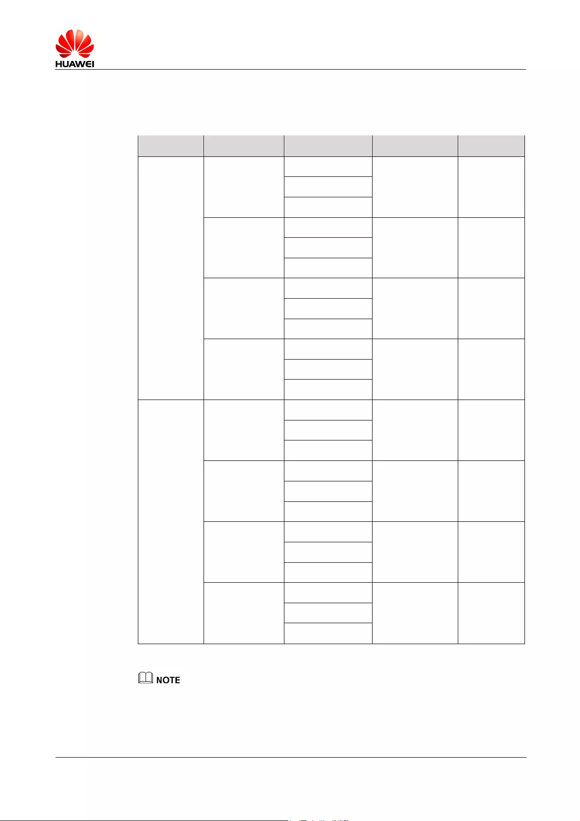
Table 11-3 Working currents in all WCDMA service scenarios
Description
Bands Current Units TX power (dBm)
WCDMA
Band
I(W2100) 200
mA
1
230
10
400
22
Band II
(W1900) 200 mA
1
230 10
300 22
Band
V(W850) 200 mA
1
240 10
350 22
Band
VIII(W900)
200
mA
1
240
10
380
22
HSDPA
Band
I(W2100) 220
mA
1
250
10
410
22
Band II
(W2100) 220 mA
1
250 10
330 22
Band
V(W850) 220 mA
1
250 10
380 22
Band
VIII(W900)
220
mA
1
250
10
410
22
Values in Table 11-3 are average values obtained from a certain number of test samples.
MS2131
Hardware Design Guide
Appendix
Issue 02 (2017-1-13) Huawei Proprietary and Confidential
Copyright © Huawei Technologies Co., Ltd.
42
11.2 Appendix Two MS2131 OTA Data
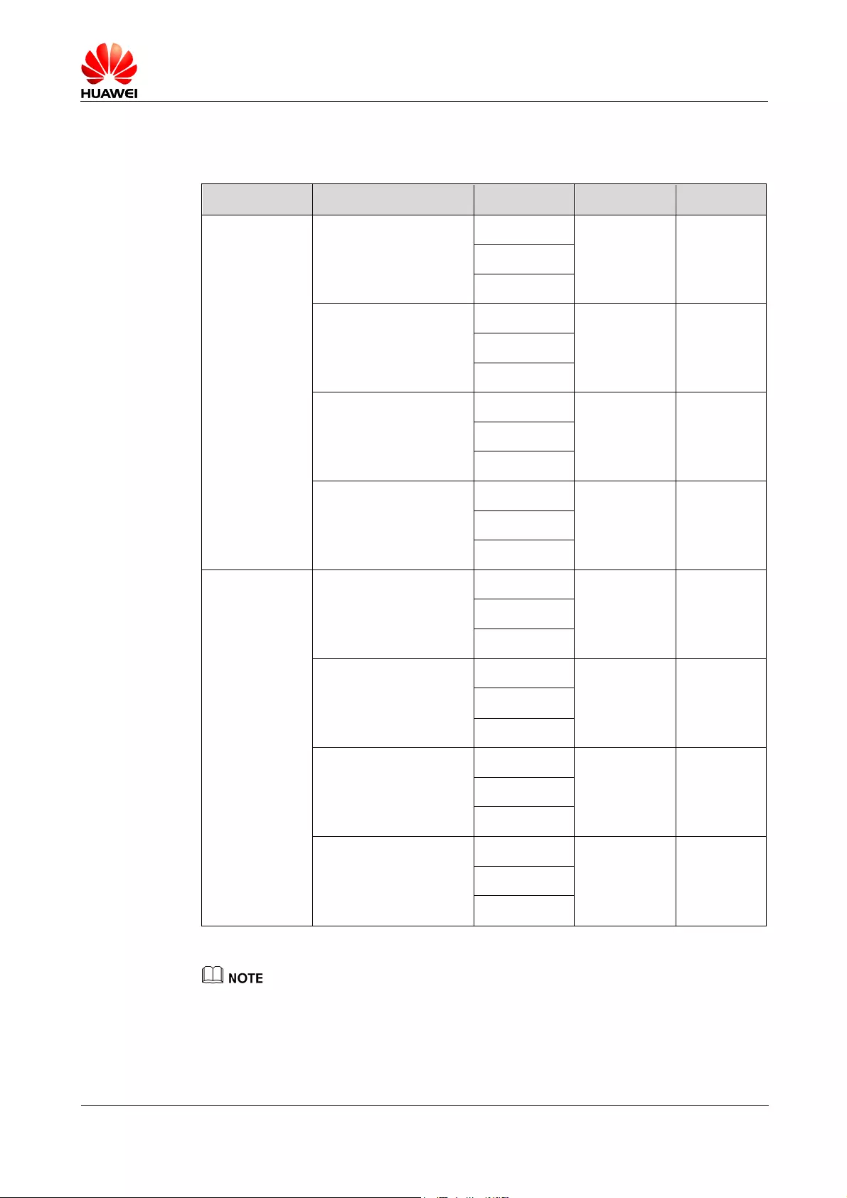
Table 11-4 MS2131 TIS
Description
Bands Channel Test Value Units
WCDMA
Band I(W2100)
10562
-104
dBm
10700
10838
Band II
(W1900) 9662
-104
dBm
9800
9938
Band V(W850)
4357
-103
dBm
4408
4458
Band
VIII(W900) 2937
-102
dBm
3012
3088
GSM
GSM 850
128
-102
dBm
190
251
GSM 900
975
-102
dBm
37
124
GSM 1800
512
-103
dBm
698
885
GSM 1900
512
-103
dBm
661
810
Values in Table 11-4 are average values obtained from a certain number of test samples, which are tested
in the stacking conditions shown in Figure 5-2. The tests are implemented with a PC. If the stacking fails
to meet requirements made in section 5.4 "Antenna Design Requirements", the MS2131 performance
may worsen compared with data in Table 11-4.
MS2131
Hardware Design Guide
Appendix
Issue 02 (2017-1-13) Huawei Proprietary and Confidential
Copyright © Huawei Technologies Co., Ltd.
43
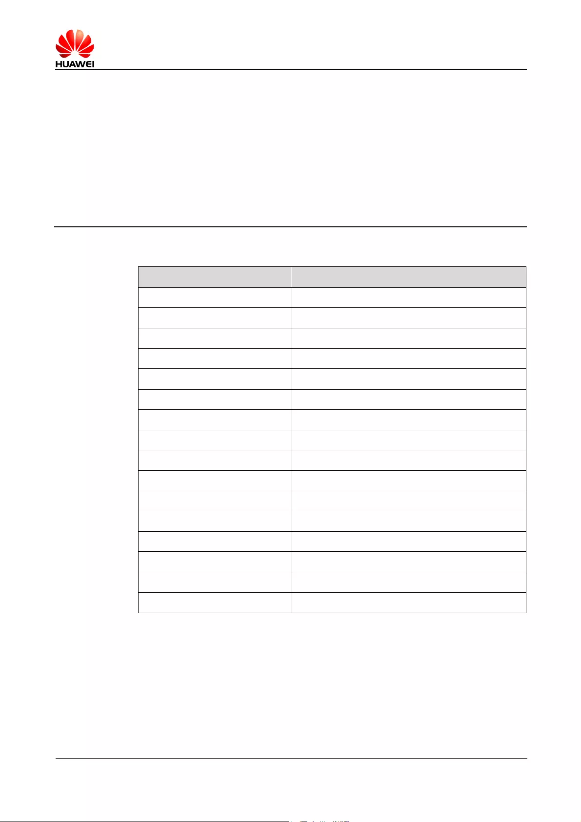
Table 11-5 MS2131 TRP
Description Bands Channel Test Value Units
WCDMA
Band I(W2100)
9612
19
dBm
9750
9888
Band II (W1900)
9662
14
dBm
9800
9938
Band V(W850)
4132
19.5
dBm
4183
4233
Band VIII(W900)
2712
19.5
dBm
2787
2863
GSM
GSM 850
128
27.5
dBm
190
251
GSM 900
975
29
dBm
37
124
GSM 1800
512
24
dBm
698
885
GSM 1900
512
23.5
dBm
661
810
The preceding values are average values obtained from a certain number of test samples. Figure 5-2
shows the MS2131 deployed in a PCB. Samples are tested deployed in the board. If the PCB is not
designed as required in section 5.4 "Antenna Design Requirements", the MS2131 performance may
worsen compared with data in Table 11-4.
MS2131
Hardware Design Guide
Acronyms and Abbreviations
Issue 02 (2017-1-13) Huawei Proprietary and Confidential
Copyright © Huawei Technologies Co., Ltd.
45
A Acronyms and Abbreviations
Acronym or Abbreviation Expansion
CDMA Code Division Multiple Access
DL Down link
DTE Data Terminal Equipment
EDGE Enhanced Data Rate for GSM Evolution
EMI Electro Magnetic Interference
ESD Electro- Static discharge
GND Ground
GPIO General-purpose I/O
GPRS General Packet Radio Service
GPS Global Positioning System
GSM Global System of Mobile communication
HSDPA High Speed Downlink Packet Access
NC Not connected
PCM Pulse-code modulation
USB Universal Serial BUS
WCDMA Wideband CODE division multiple access
